SELF ASSEMBLED ONE DIMENSIONAL NANOSTRUCTURES ON Si (001) SURFACES
NANOESTRUCTURAS UNIDIMENSIONALES AUTOENSAMBLADAS EN SUPERFICIES DE Si (001)
Gregorio H. Cocoletzi1 and Noboru Takeuchi 2
1Instituto de Física, Universidad Autónoma de Puebla, Apartado Postal J–48, Puebla 72570, México
2Centro de Ciencias de la Materia Condensada, Universidad Nacional Autónoma de México, Apartado Postal 2681, Ensenada, Baja California, 22800, México
Contacto: Noboru Takeuchi takeuchi@cnyn.unam.mx
(Recibido: 06/2011. Aceptado: 08/2011)
Cómo citar: Cocoletzi, G.H, & Takeuchi, N., Momento, 43, 1 (2012)
Abstract
Different kinds of one dimensional nanostructures that self assemble on semiconductor surfaces have been studied experimental and theoretically in recent years. They are interesting not only because of possible applications but also from a fundamental point of view. In basic research the interest is motivated by the possibility to understand interesting physical phenomena that are related to these systems, such as surface stability, growth, and the properties of one–dimensional systems, to mention only a few. For technological applications, they are very important in nanoelectronics, since there is always a search for ways of creating smaller circuits (in the lower tens of nanometers), beyond the capabilities of normal lithography. In this article, we survey some of such systems when grown on the Si(001) surface.
Keywords: Dimensional nanostructure, silicon, surface.
Resumen
Diferentes tipos de nanoestructuras unidimensionales que pueden autoensamblarse en superficies de semiconductores se han estudiado experimental y teóricamente en los últimos años. Estos sistemas son interesantes no sólo por sus posibles aplicaciones, sino también desde un punto de vista fundamental. En la investigación básica el interés está motivado por la posibilidad de comprender interesantes fenómenos físicos que están relacionados con estos sistemas, tales como estabilidad de la superficie, el crecimiento y las propiedades de los sistemas de una sola dimensión, para mencionar sólo unos pocos. Para las aplicaciones tecnológicas, son muy importantes en la nanoelectrónica, ya que siempre hay una búsqueda de métodos para fabricar circuitos más pequeños (por debajo de las decenas de nanómetros), más allá de las capacidades de litografía normal. En este artículo haremos una revisión de algunos de estos sistemas, crecidos en la superficie Si(001).
Palabras clave: Nanoestructura unidimensional, silicio, superficie.
Introduction
The study of self assembled nanostructures is the topic of active research since it has the potential of being used in the fabrication of nanometer scale electronic devices. The size of the integrated circuits is becoming smaller and smaller, and today, the dimensions of the transistors are on the scale of tens of nanometers. To continue with this trend, and being able to follow Moore's law, which says that the amount of space required to install a transistor on a chip shrinks by roughly half every year and half, we may need to fabricate devices of just few nanometers size. Since conventional lithography is reaching their limits at around 10–15 nm, other methods are needed [1]. Nanolitography methods, based on scanning probe microscopies are very slow, and they are diffcult to implement at large scales. Another approach is the growth of self–assembled nanostructures, using the principle that the atoms and molecules will always seek the lowest energy level available to them. Over the last couple of decades, different systems which results in self assembled one dimensional (1D) nanostructures on semiconductors surfaces have been studied. In this review, we will focus on the formation of 1D nanostructures on the (001) surface of silicon, which is the technological most relevant surface. In particular we will discuss the formation of single atom wide lines of group III and IV metal on Si(001) surfaces, and the grow of organic 1D nanostructures on the same surfaces. The paper is organized as follows: In Section II we describe the methods. In Section III we describe the substrate: clean and hydrogenated Si(001) surfaces, in Section IV present results of single atom wide lines on Si(001) surfaces, in Section V we show the formation of Rare Earth silicides one dimensional nanostructures on Si(001) surfaces, in Section VI we discuss the formation of Organic 1D nanostructures on hydrogenated Si(001) surfaces, and in section VII we present the conclusions.
Method
Calculations have been performed using the periodic density functional theory (DFT) [2, 3], as implemented in the Quantum ESPRESSO package [4]. Exchange and correlation energies are modeled according to the local density approximation (LDA) [5] or the generalized gradient approximation (GGA) with the Perdew–Burke–Ernzerhof (PBE) gradient corrected functional [6]. Electron–ion interactions are treated within the pseudopotential method [7], while the electron wave functions are expanded in plane waves. To model the Si(001) surface, a repeated slab geometry was used, with each slab consisting of five Si layers and the adatoms on the top surface. Dangling bonds at the bottom surface were saturated by hydrogen atoms. The bottom Si layer and the saturating H atoms were frozen in order to simulate a bulk–like environment. Two consecutive slabs were separated by an empty space ~9.0 Å wide to reduce slab–slab interactions.
The substrate: clean and hydrogenated Si(001) surfaces
A. The substrate: clean and hydrogenated Si(001) surfaces
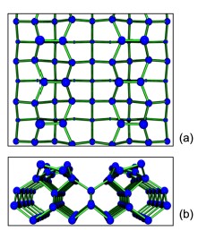
The ideal bulk terminated Si(001)–(1×1) surface is not stable since it leaves two unsaturated dangling bonds [8]. Instead, surface atoms rearrange themselves forming dimers, reducing the number of dangling bonds/(surface atom) to one. There is an additional charge transfer from one of the Si atoms (which moves down) to the other atom of the dimer (which moves up). In this way all the surface dangling bonds are saturated and the surface is stable. The asymmetric Si dimers can have different orientations. The most stable configuration corresponds to Si dimers oriented in opposite orientations along and perpendicular to the Si dimer rows, and therefore having a c(2×4) periodicity (Fig. 1).
The electronic band structure of the Si(001) surface shows both occupied and unoccupied surface states situated within the gap region. The highest occupied surface state is localized on the upper dimer atom, while the lowest unoccupied surface state is localized on the lower dimer atom.
B. Hydrogen covered Si(001) surfaces
Adsorption of hydrogen on the Si(001) surface leads to different structures, depending on the H coverage and preparation procedures. At least three different H–induced reconstructions could occur: H–Si(001)(1×1), H–Si(001)(2×1), and H–Si(001)(3×1) [9, 10].
For the H–Si(001)–(2×1) monohydride structure, the hydrogen coverage is one monolayer (1ML), all dimer Si dangling bonds being saturated by a H atom. No Si–Si dimer bond is broken, and all dimers become symmetric as seen in Figs. 2a and 2b. On the H–Si(001)–(3×1) surface all Si dangling bonds are also saturated, but the hydrogen coverage is 4/3, and two different sub–units can be observed. Figures 2c and 2d show schematic top and side views of the fully relaxed H–Si(001)–(3×1) surface. The first sub–unit is similar to the one observed in the (2×1)surface and it consists of H–terminated symmetric Si dimers; the second is a SiH2 dihydride unit (also called a monomer). For the H–Si(001)(1×1) surface, the hydrogen coverage is 2 monolayers (2 ML), all Si dimers are broken, and the two dangling bonds of each Si atom are saturated by hydrogen atoms forming a SiH2 dihydride unit. Figures 2e and 2f show schematic top and side views of the surface. It can be seen that after fully relaxing the atomic positions, a canted–row dihydride structure was found [9, 10] the total energy was lowered by a small rotation of the SiH2 groups. This rotation increases the distance between H atoms in neighboring dihydrides to 2.22 Å and in this way it decreases the repulsive interactions between SiH2 groups.
Figure 1. Schematic structure of the c(2×4) reconstruction of the Si(001) surface. a) Top view. Larger circles represent atoms closer to the surface. b) Side view.
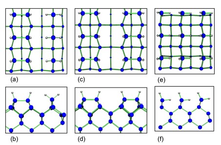
Figure 2. Schematic structures of the (3×1), (2×1) and (1×1) hydrogenated Si(001) surfaces. (a) Top, and (b) side views of H–Si(001)–(2×1). (c) Top, and (d) side view of H–Si(001)–(3×1). (e) Top, and (f) side views of H–Si(001)–(1×1). Big blue circles correspond to Si atoms, while small gray circles represent H atoms.
Single atom wide lines on Si(001) surfaces
Scanning tunneling microscopy (STM) experiments have shown that when a small fraction of a monolayer of group III metals, Al, Ga, or In is deposited on Si(001) at room temperature and in ultra high vacuum (UHV), there is a formation of lines of ad–dimers on the surface. These lines have been also observed for Sn and Pb on Si(001) and can be considered as truly one–dimensional systems since they are one atom wide and one atom high.
Early studies of the adsorption of Ga on Si(001) have suggested that the diffusion of Ga on this surface may be anisotropic [11]. Later STM experiments showed that in UHV and at room temperature [12], Ga forms lines of adatom dimers on the surface, and that these lines run in a direction perpendicular to the underlying Si dimer rows. Increasing the coverage results in the crowding of these lines and at 0.5 ML Ga forms an ordered (2×2) phase [13]. Similar lines were later found for Al [14], In [15] (Fig. 3), Sn [16], and Pb [17].

Figure 3. High resolution STM filled state image of In lines on Si(001). The inset shows greater detail. Courtesy of Prof. J. Nogami, U. Toronto.
The atomic structure of the one dimensional lines formed by group III atoms is shown schematically in Fig. 4. First principles calculations have shown that these lines are indeed formed by ad–dimers: dimer formation was more favorable that adsorption of two separated adatoms by 1.2 eV for Al [18] and Ga [19], and 1.0 eV for In [19]. In the most stable configuration, the symmetric ad–dimers are oriented parallel to the Si dimers and they are located in the trenches between two Si dimer rows [19]. Once a dimer is formed, a third atom will bind at a site adjacent to the dimer.
This site is more reactive than others since adsorption there does not require a breaking of a Si π bond. A fourth atom will form a dimer with the third one, and this process can go on, resulting in the formation of the one dimensional lines. Brocks, Kelly and Car has called it a surface polymerization reaction [18]. Another way

Figure 4. Schematic structures of the formation of group III 1D lines on Si(001–c(2×4). (a) Top, and (b) side views. Blue circles correspond to Si atoms, while larger gray circles represent Al atoms.
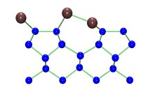
Figure 5. Side view of the schematic structure of the 1D lines of Pb on Si(001). Blue (dark red) circles represent Si (Pb) atoms.
to understand this process is by counting the number of dangling bonds left at each step of the process. When a single ad–dimer attaches to the surface, four Si dimers (eight atoms) are involved in the adsorption. Four of these eight Si atoms form bonds with the ad–dimer, leaving four Si unpaired electrons per ad–dimer. If the

Table 1. Calculated bond lengths (in Å) for the (001) surface of Si covered by different coverages of group III and IV metals
next dimer is adsorbed adjacent to the first one, there is no increase in this number. However, if the dimer is adsorbed somewhere else, the number of unpaired electrons will double.
Similar results have been found for Sn [16] and Pb [17[ on Si(001). However, for group IV atoms, as seen in Fig. 5, the ad–dimers are asymmetric: the two atoms in the dimers do not have the same vertical position [20, 21]. This is not surprising since an in the case of the clean Si(001) surface, this asymmetry is due to the electronic structure: each Pb atom has four valence electrons. Two of them saturate the dangling bonds of the Si surface, another is use form the Pb–Pb dimer, and there is a remaining electron in each Pb atom of the dimer. To lower the energy, there is a charge transfer from one atom who is pushed down, to the other which moves up. The two electrons in the up Pb atom form a lone pair, which is also stable. In all cases, increasing the coverage up to 0.5 ML, a (2×2) structure is formed. However, as shown in Table 1, the structural parameters of the surface change little in a single ad–dimer, one dimensional line, and two dimensional (2×2) reconstruction.
Rare Earth silicides on Si(001) surfaces
The lines mentioned in last section are unstable against anneling and they reorganize to form more compact configurations: a (4×3) reconstruction for In/Si(001) [23–25], and Al/Si(001) [26, 27], and a c(4×8) for Sn [16, 28] and Pb on Si(001) [29, 30]. A more hopeful method for the formation of 1D nanostructures on Si(001) is the growth of rare–earth silicides.
In this section, we concentrate in the 1D lines formed by rare earth (RE) and transition metals grown on Si(001) surfaces. The reason to choose RE is because these elements display good conductivity and low Schottky barrier when they are deposited on silicon surfaces, which are good characteristics for technological applications. Although Sc and Y are not RE elements, they share some of the RE elements properties. Likewise scandium and yttrium silicides possess similar characteristics to the rare earth silicides. Our interest is to describe epitaxial self–assembled silicide 1D line growth on Si(001). This is possible because the magnitude of the lattice mismatch between the epilayer and the substrate is large along one crystal axis and small along the perpendicular axis, yielding self–assembled 1D structures. Those stable compounds that satisfy these requirements for assembling 1D quantum structures on Si(001) are: TmSi2, ErSi2, YSi2, HoSi2, DySi2, TbSi2, GdSi2, ScSi2, and SmSi2. We shall illustrate some specific examples on the construction of 1D nanostructures deposited on the Si(001) surface. Recent reports [31] on the deposition ScSi2, ErSi2, DySi2, and GdSi2 have demonstrated that the use of the self–assembly method may allow the construction of 1D nano–structures. The lattice mismatches of ScSi2, ErSi2, DySi2, and GdSi2 are: –4.6, 6.3, 7.6, and 8.9 %, respectively, along one of the Si ⟨110⟩ directions and mismatches of: 0.8, –1.6, –0.1, and 0.8%, respectively, along the perpendicular Si ⟨110⟩ direction.
The experiments we shall describe [31], account for a clean Si(001) substrate, which displays slopes downward along the [110]Si direction, with terraces of different heights. The average terrace width along [110]Si is 578 Å and along ![]() is 213 Å. The assembling of 1D nanostructures on the at Si(001) substrates were done at 600°C for 2 min. obtaining coverages of approximately 0.35 ML Sc, 0.20 ML Er, 0.25 ML Dy, and 0.28 ML Gd. Following the deposition, the samples were annealed at 600°C for 2 more min. obtaining 1D nanostructures aligned along one of the two perpendicular [110]Si directions. One–dimensional nano–structures were observed on all four samples. The 1D lines are straight and do not follow or terminate at single Si atomic steps, but rather the steps have zig-zag pattern with step bunching that locally follow the 1D nanostructure. The widths and heights of the 1D nanostructure varied significantly because of their different lattice mismatches with respect to the silicon substrate. The average dimensions were measured from STM images. According to Fig. 4 of Ref. [31], the average width versus the large–lattice–mismatch (%) is as follows: the smallest 1D nanostructure width corresponds to GdSi2 and the largest to ScSi2 along the
is 213 Å. The assembling of 1D nanostructures on the at Si(001) substrates were done at 600°C for 2 min. obtaining coverages of approximately 0.35 ML Sc, 0.20 ML Er, 0.25 ML Dy, and 0.28 ML Gd. Following the deposition, the samples were annealed at 600°C for 2 more min. obtaining 1D nanostructures aligned along one of the two perpendicular [110]Si directions. One–dimensional nano–structures were observed on all four samples. The 1D lines are straight and do not follow or terminate at single Si atomic steps, but rather the steps have zig-zag pattern with step bunching that locally follow the 1D nanostructure. The widths and heights of the 1D nanostructure varied significantly because of their different lattice mismatches with respect to the silicon substrate. The average dimensions were measured from STM images. According to Fig. 4 of Ref. [31], the average width versus the large–lattice–mismatch (%) is as follows: the smallest 1D nanostructure width corresponds to GdSi2 and the largest to ScSi2 along the ![]() direction, with values between 4 and 10 nm. Likewise the smallest 1D nanostructure width corresponds to GdSi2 and the largest to ScSi2 along the [100] direction, with values between 50 and 110 Å. The 1D quantum structures of ErSi2 and DySi2 have average values between these upper and lower limits. The average height versus the large–lattice–mismatch (%) is as follows: the smallest 1D nanostructure height corresponds to GdSi2 and the largest to ScSi2 along the
direction, with values between 4 and 10 nm. Likewise the smallest 1D nanostructure width corresponds to GdSi2 and the largest to ScSi2 along the [100] direction, with values between 50 and 110 Å. The 1D quantum structures of ErSi2 and DySi2 have average values between these upper and lower limits. The average height versus the large–lattice–mismatch (%) is as follows: the smallest 1D nanostructure height corresponds to GdSi2 and the largest to ScSi2 along the ![]() , with values between 0.25 and 1.5 nm. Likewise the smallest 1D nanostructure height corresponds to GdSi2 and the largest to ScSi2 along the [110], with values between 5 and 30 Å. The 1D nanostructures of ErSi2 and DySi2 have average height values between these two limits. Finally, the average height as function of the small–lattice–mismatch (%) shows different features, no monotonic behavior is observed along both
, with values between 0.25 and 1.5 nm. Likewise the smallest 1D nanostructure height corresponds to GdSi2 and the largest to ScSi2 along the [110], with values between 5 and 30 Å. The 1D nanostructures of ErSi2 and DySi2 have average height values between these two limits. Finally, the average height as function of the small–lattice–mismatch (%) shows different features, no monotonic behavior is observed along both ![]() and [110] directions, the height average is of the order of hundreds of nanometers, except for ScSi2, which is of the order of 500 Å. The size and shape of the self–assembled 1D nanostructures are strongly dependent on their asymmetric lattice mismatches with respect to the Si lattice. All the RE, Sc and Y silicides we have considered have the AlB2 hexagonal crystal structure.
and [110] directions, the height average is of the order of hundreds of nanometers, except for ScSi2, which is of the order of 500 Å. The size and shape of the self–assembled 1D nanostructures are strongly dependent on their asymmetric lattice mismatches with respect to the Si lattice. All the RE, Sc and Y silicides we have considered have the AlB2 hexagonal crystal structure.
A model of the crystallographic geometry of the silicide thin films with respect to the Si(001) substrate and the interfacial structures have been recently proposed [32]. The model was illustrated by describing the relative orientation of the bulk atomic geometries of the silicide and silicon in the deposition of ErSi2 on the Si(001) surface [32]. For this example, the ErSi2 and Si bulk structures and their crystallographic orientation relationship are as follows: When the ErSi2 is bonded to Si(001), the Si atom in ErSi2 could replace those of on Si(001). Such a bonding configuration maintains the bulk-like Si–Si bonds on both ErSi2 and Si sides of the interface. However, there exist a direction dependence on the atomic distances between silicon atoms in ErSi2 along the ![]() ErSi2 direction and the [0001]ErSi2 direction, which are 3.79 Å and 4.09 Å in bulk, respectively. These values are different from that of bulk atomic distance 3.84 Å between silicon atoms. When ErSi2 is deposited on the Si(001) surface, the lattice mismatch strain along the [0001]ErSi2 axis increases much faster than that along
ErSi2 direction and the [0001]ErSi2 direction, which are 3.79 Å and 4.09 Å in bulk, respectively. These values are different from that of bulk atomic distance 3.84 Å between silicon atoms. When ErSi2 is deposited on the Si(001) surface, the lattice mismatch strain along the [0001]ErSi2 axis increases much faster than that along ![]() ErSi2 . To minimize the strain energy, the ErSi2 crystal grows preferentially along the
ErSi2 . To minimize the strain energy, the ErSi2 crystal grows preferentially along the ![]() ErSi2 direction. According to this model the '2×1' dimer rows on the Si(001) surface are oriented along the
ErSi2 direction. According to this model the '2×1' dimer rows on the Si(001) surface are oriented along the ![]() Si direction by the pairing of dangling bonds. In this way the dimer rows are perpendicular to the 1D nanostructures grown on the same terrace. Lattice mismatches of ScSi2, ErSi2, DySi2, and GdSi2 have different values, but the differences are not large. Therefore, it is not surprising to find that the minimization of the strain energy in silicide crystals deposited on Si(001) takes place, when the growth is preferentially along the direction, leading to the formation of elongated silicide 1D nanostructure
Si direction by the pairing of dangling bonds. In this way the dimer rows are perpendicular to the 1D nanostructures grown on the same terrace. Lattice mismatches of ScSi2, ErSi2, DySi2, and GdSi2 have different values, but the differences are not large. Therefore, it is not surprising to find that the minimization of the strain energy in silicide crystals deposited on Si(001) takes place, when the growth is preferentially along the direction, leading to the formation of elongated silicide 1D nanostructure
Scanning tunneling microscopy (STM) and low–energy electron diffraction studies have demonstrated that epitaxial growth of Y at less than 1 monolayer (ML) (4×2(–surface reconstruction were obtained with some features of (6×2) periodicity. At higher coverage Y formed either islands or 1D nanostructures depending on the heating and annealing conditions, while the substrate presented a (3×1) periodicity structure. STM investigations of the deposition of ScSi on Si(001) have also very recently reported. High quality at Si(001) substrates were prepared, which showed terraces along and of different heights. A deposition of a few seconds up to 7 min of rare earth elements on Si(001) yielded up to ~0.5 ML. After a deposition the samples were annealed for a few minutes. A (2×1) reconstructed surface structure is obtained on Si(001) terraces between single atomic steps. An image of STM of ScSi2 grown on at Si(001) substrates is displayed in Fig. 1 of [31]. It is clearly seen the slopes of the substrate downward from top right to bottom left with the terraces displaying different heights and separated by atomic steps, but many steps can be observed near the ends of the 1D line. The 1D–nano–structures are aligned along one of the two perpendicular ⟨110⟩Si directions.
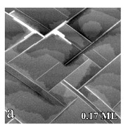
Figure 6. STM image showing the formation of lines on Si(001) after the deposit of 0.17 ML of DySi2. Courtesy of Prof. J. Nogami, U. Toronto.
As mentioned before 1D nanostructures self–assemble in uniaxially mismatched systems. Examples of those systems are RE silicides, which are deposited on Si(001). It is also important to point out the existence of an alternative surface morphology that may be used to construct 1D nanostructures. We shall mention the deposition of RE silicides (DySi2, GdSi2, and ErSi2)[33] on a single domain vicinal Si(001) surface, which yielded 1D quantum structures. In these experiments parallel 1D nanostructures were produced, together with compact silicide islands as seen in Fig. 6. The formation of 1D lines was controlled by manipulating the growth kinetics, or by judicious choice of the RE metal. The deposition of DySi2, GdSi2, and ErSi2 on the substrate showed that the growth of 1D nanostructures of Gd may be achieved over a wider range of conditions than other metals. The single domain vicinal Si(001) surface is tilted 4° off towards Si![]() , resulting in a double step spacing of 39 Å. All the steps are perpendicular to the Si dimer row direction, and all Si dimers are parallel to the step edge. In this way the structure shows a typical area of the surface with less than 5% minority dimer orientation, due to local splitting of the double–height steps. Since the 1D nanostructures are formed perpendicular to the Si dimer row direction on the substrate, they would grow parallel to the step edges on the vicinal surface.
, resulting in a double step spacing of 39 Å. All the steps are perpendicular to the Si dimer row direction, and all Si dimers are parallel to the step edge. In this way the structure shows a typical area of the surface with less than 5% minority dimer orientation, due to local splitting of the double–height steps. Since the 1D nanostructures are formed perpendicular to the Si dimer row direction on the substrate, they would grow parallel to the step edges on the vicinal surface.
Organic 1D nanostructures on hydrogenated Si(001) surfaces
There is a current interest in attaching organic molecules to silicon surfaces, because it offers the possibility of combining the richness of organic chemistry with the mature semiconductor technology, increasing in this way the possible applications of silicon [34–45]. In particular, the attachment of organic molecules in silicon surfaces could be used as a basic component of electronic devices, or as to connect nanoscale electronic devices. A promising approach to grow organic nanostructures in silicon surfaces is a radical–initiated reaction of terminally unsaturated molecules with hydrogen–terminated Si surfaces with dangling bonds. This process has been recently applied to grow organic nanostructures on H–Si(111) [37, 38], H–Si(001)–(2×1) [39–43], and H–Si(001)–(3×1) surfaces [43, 44]. On H–Si(001) surfaces this technique has allowed the fabrication of 1D molecular lines oriented in different directions [39–43]. The deposit of Styrene molecules on the H–Si(001)–(2×1) results in the formation of 1D lines along the Si dimer rows [39–43] as shown in Fig. 7, while on the H–Si(001)–(3×1) surface the formation of similar one dimensional structures has been also observed, but in this case, the lines are orthogonal to the Si dimer row [43, 44]. Depositing allyl mercaptan instead of styrene on H–Si(001)–(2×1) results in the formation of 1D line orthogonal to the Si dimer rows [45] (Fig. 7).
Other molecules that can be grown on Si(001) surfaces using this method are vinyl ferrocene, and long-chain alkenes (CnH2n; n ≥ 8).
Styrene on H–Si(001)–(2×1)
The proposed mechanism for the growth of styrene on H–Si(001)–(2×1) consists of two main steps. First, the styrene molecule reacts with a single Si dangling bond which was previously generated by removing a H atom from the surface. The molecule binds to the surface through a Si–C bond and gives rise to a metastable surface bound carbon–centered radical. Then, this highly reactive carbon radical abstracts a hydrogen atom from a neighboring Si–H group on the same Si dimer row to produce a new silicon dangling bond, where another molecule can be attached, thus leading to a surface chain reaction [39–43]. A first principles calculations of the reaction of styrene with hydrogenated H–Si(001)–(2×1) predicted a H abstraction barriers of 0.88 eV, larger than the desorption barrier (0.55 eV) from the metastable state, which makes the reaction unlikely [41].

Figure 7. STM image of the H–Si(001)–(2×1) surface containing a small concentration of dangling bonds exposed to allyl mercaptan and styrene.
In a more recent first principles calculations, several metastable structures were found [42]. In these configurations, all Si dangling bonds are saturated, but the breaking of the π bond between the styrene carbon α and β atoms results in a radical. Figs. 8(a) and (b) shows two such structures with the phenyl group oriented perpendicular to the surface. In the structure shown in Fig. 8 a, the plane formed by the C–Si bond and the Cα–Cβ bond is parallel to the Si dimer where the molecule is attached, while in the structure show in Fig. 8 b, the same plane is perpendicular to the Si dimer. This state is the same reported in ref. [41] with a calculated adsorption energy of 0.55 eV.
Figures 8c and 8d show two additional metastable structures in which the styrene molecules are not perpendicular to the surface, but bent toward it. Such structures are more stable that the ones with the plane of the phenyl group perpendicular to the surface. Their binding energies are 0.75 and 0.77 eV respectively.

Figure 8. Metastable (C–radical containing) adsorption structures of a styrene molecule on the H–Si(001)–(2×1) surface. Energies are –0.53, –0.63, –0.66, –0.78 eV for 8a, 8b, 8c, 8d, respectively, relative to the non–interacting molecule + surface system. Big blue circles correspond to Si atoms, small gray circles represent H atoms, and red circles are C atoms.
In geometry 8c (8d) the plane formed by the C–Si bond and the Cα–Cβ bond is parallel (perpendicular) to the Si dimer where the molecule is attached, and favor growth perpendicular (parallel) to the Si dimer rows.
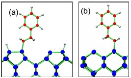
Figure 9. Schematic structures of a styrene molecule adsorbed on the H–Si(001)–(2×1) surface after hydrogen abstraction from a nearest neighbor site. In 9a the H atom has been abstracted from the next Si dimer row, while in 9b from a neighboring dimer in the same row.
Takeuchi, Selloni and Kanai also calculated the minimum energy path for Hydrogen abstraction in both cases [42]. They found activation energies larger than 1.06 eV for abstraction from the adjacent dimer row, and 0.67 eV from the same row. The final geometries are shown in Fig. 9 a and b respectively.
These results indicate that growth parallel to the dimer rows is kinetically more favorable than growth perpendicular to the dimer rows, in good agreement with experiments. The calculated energy barrier is also smaller than the results from ref. [41], and much smaller that the desorption energy, indicating that once the molecule is attached to the surface it will be more favorable to abstract the hydrogen atom and continue the reaction instead of detaching from the surface.
Takeuchi, Selloni and Kanai [42] also studied the formation of 1 dimensional organic nanostructure formed by dimethyl styrene on Si(001), finding similar activation energies. However, different from the case of styrene, they found smaller desorption barrier for the more complex dimethyl styrene molecules, explaining why such nanostructure are not observed at room temperature for dimethyl styrene.
Allyl mercaptan on H–Si(001)–(2×1)
The proposed mechanism for the growth of allyl mercaptan on H–Si(001)–(2×1) is schematically shown in Fig. 10 [45].
(a) A styrene molecule approaches the surface with a dangling bond. (b)The molecule binds to the surface through a Si–C bond, and similar to the previous surfaces, gives rise to a metastable surface bound carbon–centered radical. (c)Then, this highly reactive carbon radical abstracts a hydrogen atom from the SH group, transferring the radical previously centered at C (carbon) on S (sulfur), resulting in a thiyl radical. (d) Then, this reactive radical abstracts a hydrogen atom from the nearest dimer row, creating a new Si dangling bond. (e) There is a second hydrogen atom diffusion creating a DB in the more distant side of the dimer, (f) where another molecule can be attached, thus leading to a surface chain reaction.

Figure 10. Proposed mechanism for the growth of allyl mercaptan on H–Si(001)–(2×1)
It is believe that the distance between the intermediate radical and the anchoring site of the molecule is one factor that may determine the direction of line growth (parallel or perpendicular to the dimer rows). In this system, the length of the allyl mercaptan molecule makes it possible for the radical on the S atom (fig. 10c) to abstract the hydrogen atom from the next dimer row, leading to growth perpendicular to the dimer rows, and different from the case of styrene.
Summary
We have review the formation of self assembled one dimensional nanostructures on Si(001) surfaces. In this paper we have explained the formation of single atom wide, Rare Earth silicides, and organic nanostructure formed on Si(001). In the first case we have shown that group III and group IV elements form self assembled one dimensional lines on Si(001) in what is called a surface polymerization reaction. Locally the atoms are arranged in dimers. However, these lines are metastable and increasing the coverage or the temperature they form more complex reconstructions.
Rare earch silicedes also formed more complexed one dimensional nanostructures that are more stable than group III and IV lines, and therefore they are better candidates for possible applications. On the other hand it is also found that self assembled one dimensional organic nanostructures can be formed on hydrogenated surfaces with vacancies. They are formed through a process called chain reaction. Finally, we hoped that this paper has shown that the understanding of the atomic structure and properties of the nanostructure has been achieved by experiment and theory together.
Ackowledgements
NT thanks DGAPA project IN103512–3 and Conacyt Project 164485 for partial financial support. Calculations were performed in the DGCTIC–UNAM supercomputing center.
References
[1] W. Chen and H. Ahmed, Appl. Phys. Lett. 62, 1499 (1993).
[2] P. Hohenberg and W. Kohn, Phys. Rev. 136, B864 (1964).
[3] W. Kohn and L. J. Sham, Phys. Rev. 140, A1133 (1965).
[4] P. Giannozzi, S. Baroni, N. Bonini, M. Calandra, R. Car, C. Cavazzoni, D. Ceresoli, G. L. Chiarotti, M. Cococcioni, I. Dabo, A. D. Corso, S. de Gironcoli, S. Fabris, G. Fratesi, R. Gebauer, U. Gerstmann, C. Gougoussis, A. Kokalj, M. Lazzeri, L. Martin–Samos, N. Marzari, F. Mauri, R. Mazzarello, S. Paolini, A. Pasquarello, L. Paulatto, C. Sbraccia, S. Scandolo, G. Sclauzero, A. P. Seitsonen, A. Smogunov, P. Umari, and R. M. Wentzcovitch, J. Phys. Condens. Mat. 21, 395502 (2009).
[5] D. M. Ceperley and B. J. Alder, Phys. Rev. Lett. 45, 566 (1980).
[6] J. P. Perdew, K. Burke, and M. Ernzerhof, Phys. Rev. Lett. 77, 3865 (1996).
[7] K. Laasonen, A. Pasquarello, R. Car, C. Lee, and D. Vanderbilt, Phys. Rev. B 47, 10142 (1993).
[8] J. P. LaFemina, Surf. Sci. Rep. 16, 137 (1992).
[9] J. E. Northrup, Phys. Rev. B 44, 1419 (1991).
[10] S. Ciraci and I. P. Batra, Surf. Sci. 178, 80 (1986).
[11] K. L. Carleton and S. R. Leone, J. Vac. Sci. Technol. B 5, 1141 (1987).
[12] J. Nogami, S. il Park, and C. F. Quate, Appl. Phys. Lett. 53, 2086 (1988).
[13] B. Bourguignon, K. L. Carleton, and S. R. Leone, Surf. Sci. 204, 455 (1988).
[14] J. Nogami, A. A. Baski, and C. F. Quate, Phys. Rev. B 44, 1415 (1991).
[15] A. A. Baski, J. Nogami, and C. F. Quate, Phys. Rev. B 43, 9316 (1991).
[16] A. A. Baski, C. F. Quate, and J. Nogami, Phys. Rev. B 44, 11167 (1991).
[17] J.–Y. Veuillen, J.–M. Gomez–Rodriguez, and R. C. Cinti (AVS, 1996))pp. 1010–1014.
[18] G. Brocks, P. J. Kelly, and R. Car, Phys. Rev. Lett. 70, 2786 (993).
[19] N. Takeuchi, Phys. Rev. B 63, 035311 (2000).
[20] M. E. González–Méndez and N. Takeuchi, Phys. Rev. B 58, 16172 (1998).
[21] T.–L. Chan, C. Z. Wang, Z.–Y. Lu, and K. M. Ho, Phys. Rev. B 72, 045405 (2005).
[22] J. E. Northrup, M. C. Schabel, C. J. Karlsson, and R. I. G. Uhrberg, Phys. Rev. B 44, 13799 (1991).
[23] A. V. Zotov, A. A. Saranin, V. G. Lifshits, J.–T. Ryu, O. Kubo, H. Tani, M. Katayama, and K. Oura, Phys. Rev. B 57, 12492 (1998).
[24] O. Bunk, G. Falkenberg, L. Seehofer, J. Zeysing, R. Johnson, M. Nielsen, R. Feidenhans'l, and E. Landemark, Appl. Surf. Sci. 123–124, 104 (1998).
[25] N. Takeuchi, Phys. Rev. B 63, 245325 (2001).
[26] G. H. Cocoletzi and N. Takeuchi, Surf. Sci. 504, 101 (2002).
[27] J. Seo, J. Park, S. Jung, K.–H. Yoo, C. Whang, S. Kim, D. Choi, and K. Chae, Chem. Phys. Lett. 417, 72 (2006).
[28] J. Nogami, Private communication.
[29] G. Falkenberg, R. L. Johnson, and N. Takeuchi, Phys. Rev. B 64, 035304 (2001).
[30] R. G. Zhao, J. F. Jia, and W. S. Yang, Phys. Rev. B 48, 5333 (1993).
[31] Y. Chen, D. A. A. Ohlberg, and R. S. Williams, J. Appl. Phys. 91, 3213 (2002).
[32] Y. Chen, D. A. A. Ohlberg, G. Medeiros–Ribeiro, Y. A. Chang, and R. S. Williams, Appl. Phys. Lett. 76, 4004 (2000).
[33] B. Z. Liu and J. Nogami, J. Appl. Phys. 93, 593 (2003).
[34] D. D. M. Wayner and R. A. Wolkow, J. Chem. Soc., Perkin Trans. 2 , 23 (2002).
[35] J. M. Buriak, Chem. Rev. 102, 1271 (2002).
[36] S. F. Bent, Surf. Sci. 500, 879 (2002).
[37] R. L. Cicero, C. E. D. Chidsey, G. P. Lopinski, D. D. M. Wayner, and R. A. Wolkow, Langmuir 18, 305 (2002).
[38] N. Takeuchi, Y. Kanai, and A. Selloni, J. Am. Chem. Soc. 126, 15890 (2004).
[39] G. P. Lopinski, D. D. M. Wayner, and R. A. Wolkow, Nature 406, 48 (2000).
[40] M. Z. Hossain, H. S. Kato, and M. Kawai, J. Phys. Chem. B 109, 23129 (2005).
[41] J.–H. Cho, D.&38211;H. Oh, and L. Kleinman, Phys. Rev. B 65, 081310 (2002).
[42] N. Takeuchi, Y. Kanai, and A. Selloni, J. Phys. Chem. C 114, 3981 (2010).
[43] N. Takeuchi and A. Selloni, J. Phys. Chem. B 109, 11967 (2005).
[44] X. Tong, G. A. DiLabio, and R. A. Wolkow, Nano Lett. 4, 979 (2004).
[45] M. Z. Hossain, H. S. Kato, and M. Kawai, J. Am. Chem. Soc. 129, 3328 (2007).