DISEÑO Y FABRICACION DE UN MICROSISTEMA PARA LA MANIPULACION DE OBJETOS BIOLOGICOS
Palabras clave:
Dilectroforesis, manipulación de micropartículas, circuitos integrados (es)La micromanipulación de partículas biológicas es una operación frecuente en medicina y microbiología, y se ha dedicado una gran cantidad de trabajo para desarrollar técnicas de manipulación mas rápidas, baratas y eficientes. En este sentido, la tecnología de microsistemas juega un papel importante ya que se puede utilizar para fabricar manipuladores de micropartículas. En este artículo se describe el diseño y fabricación de un microsistema para la manipulación de objetos biológicos, basado en el efecto dielectroforetico. También se discute la selección de la alternativa tecnológica mas adecuada dentro de las disponibles. El diseño propuesto, es un microsistema completo que incluye interfases eléctrica, óptica y fluidica, y se desarrolló empleando oro y platino como metales para los electrodos, micro mecanizado del silicio y técnicas de fotocurado de resinas fotosensibles. De la misma forma se describe la estructura de los microelectrodos desarrollados al igual que el circuito integrado resultante.
DESIGN AND FABRICATION OF A MICROSYSTEM TO HANDLE BIOLOGICAL OBJECTS
DISEÑO Y FABRICACION DE UN MICROSISTEMA PARA LA MANIPULACION DE OBJETOS BIOLOGICOS
FLAVIO
HUMBERTO FERNÁNDEZ MORALES
Ingeniero electrónico, Doctor en Electrónica,
Universidad Pedagógica y Tecnológica de Colombia, flaviofm1@gmail.com
JULIO ENRIQUE
DUARTE
Licenciado en Física, Doctor en
Física, Universidad Pedagógica y Tecnológica de Colombia, julioenriqued1@gmail.com
JOSEP
SAMITIER MARTÍ
Licenciado en física, Doctor en física, universitat de Barcelona, samitier@el.ub.es
Recibido para revisar Abril 19 de 2007, aceptado Noviembre 31 de 2007, versión final Febrero 05 de 2008
RESUMEN: La micromanipulación de partículas biológicas es una operación frecuente en medicina y microbiología, y se ha dedicado una gran cantidad de trabajo para desarrollar técnicas de manipulación mas rápidas, baratas y eficientes. En este sentido, la tecnología de microsistemas juega un papel importante ya que se puede utilizar para fabricar manipuladores de micropartículas. En este articulo se describe el diseño y fabricación de un microsistema para la manipulación de objetos biológicos, basado en el efecto dielectroforetico. También se discute la selección de la alternativa tecnológica mas adecuada dentro de las disponibles. El diseño propuesto, es un microsistema completo que incluye interfases eléctrica, óptica y fluidica, y se desarrolló empleando oro y platino como metales para los electrodos, micro mecanizado del silicio y técnicas de fotocurado de resinas fotosensibles. De la misma forma se describe la estructura de los microelectrodos desarrollados al igual que el circuito integrado resultante.
PALABRAS CLAVE: Dilectroforesis, manipulación de micropartículas, circuitos integrados
ABSTRACT: Biological particle microhandling is a common operation in medicine and microbiology, and a lot of research work has been addressed to develop faster, cheaper and more efficient manipulation techniques. In this way, microsystem technologies play an important role because they can be used to fabricate microparticle manipulators. This paper describes the design and fabrication of a microsystem to handle biological objects, based on the dielectrophoretic effects. The development of the right technological option among the possibilities at disposal is also discussed. The proposed design, a whole microsystem including electrical, optical and fluidic interfaces, was developed employing gold and platinum metals, silicon micromachining, and photoresin patterning techniques. Furthermore, the structure of the utilized microelectrode arrays, as well as the resulting microchip are also reported.
KEYWORDS: Dielectrophoresis, microparticle manipulation, integrated circuits
1. INTRODUCTION
Microsystems have gained a huge preponderance as a technology that suits very well the requirements of miniaturized sensors and actuators in industry applications. Thus, devices as accelerometers, pressure microsensors,
microfluidic components or even micromirrors are now a common approach[1-9]. Besides this, devices aimed to handle biological objects in order to obtain more confident, faster and cheaper biochemical assays have also gained attention[10-14].
Among these tools, biochips based on microelectrodes to generate inhomogeneous electric fields have been used to study and manipulate animal and plant cells, viruses, bacteria and DNA fragments[15-21].
The lateral motion of dielectric particles based on nonuniform electric fields is called common dielectrophoresis (c-DEP) [22-29]. Furthermore, if a rotary electric field is applied it can induce a rotational moment on the particle and this spin has been termed electrorotation (ROT) [30-35].
The third effect is travelling wave dielectrophoresis (TWD), and it is generated by the interaction between a travelling wave of electric field with a neutral particle suspended in it[36-40]. The mentioned three effects of electric fields actuating onto neutral matter are quite important in microsystems devoted to handle microparticles because they only require the integration of small electrodes on a substrate.
Diverse materials and technological approaches have been used to fabricate these microtools. As an example it can be mentioned silicon or glass substrates with electrodes made in gold, platinum, aluminum or ITO, which are patterned by common photolithographic processes and by laser ablation[41-45]. However, one of the main problems is the implementation of a microcavity to contain the suspension at issue because it usually requires additional development efforts, which increase the cost and complexity of the technological processing.
This article deals with the development of a microsystem addressed to bioparticle microhandling, based on the dielectrophoretic effects. The device was fabricated employing a silicon substrate onto which gold or platinum microelectrodes were grown by photolithography and lift-off techniques.
The microcavity was shaped employing a photosensitive resin, which facilitates the fabrication process. Furthermore, silicon micromachining was utilized to configure the inlet and outlet ports to allow the liquid flow through the microstructure. In the sequel, the design and fabrication process, as well as the resulting microchip are described.
2. METHODS AND MATERIALS
As previously mentioned, the main goal of this run was the development of a whole microsystem fabricated by silicon technologies, hinging on the diverse dielectrophoretic phenomena (c-DEP, ROT and TWD) in order to carry out different bioelectronic experiments such as characterization, separation and motion of microparticles, and culture of micro-organisms under the influence of strong electric fields.
It must be stressed that the experimental phase of a research work involving particle microhandling combines different subjects such as chemistry for particle preparation and suspending medium calibration, fluidics for sampling delivering and recirculation through the microchamber, optics to observe and characterize the particle electrokinetic behavior, and electronics to generate the driving signals, as well as to control the apparatus implicated in the experimental set-up. As a consequence of this, a minute design and fabrication of the microstructure is demanded because there are a lot of variables that can alter the final results.
Especially, one must keep in mind that the typical read out of this approach is done mainly by optical tools (microscopes, image analysis, etc.) rather than by electrical apparatus[46]. Also, further effort must be addressed to forming a true microchamber by patterning the walls of a cavity with a known volume, i.e. a micropool should be fabricated to guarantee a constant volume of the suspending medium over the electrodes, avoiding possible experimental fluctuations due to this item.
In view of the previously mentioned considerations, a whole microsystem was designed and fabricated as described underneath.
2.1 The proposed microsystem
Figure 1 depicts a cross section view of the proposed
device, which includes a glass or silicon substrate onto which electrodes are
grown. Moreover, this substrate can be attacked to shape the fluid flow ports
employing silicon micromachining techniques, which has been devised to sculpt
three-dimensional objects in silicon or glass substrates[47]. Holes patterned
by this technique will serve to bring the suspending medium onto the electrode
surface and once the desired measurements have been done, carry away the mixture
to further analysis if necessary. They can also be employed to permanently
recirculate the sample in order to refresh the suspending medium, bringing
new specimens over the active electrode test area, which is advantageous when
working with biological objects.
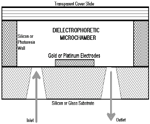
Figure 1. Cross section view
of the proposed microdevice. In this sketch three main components may be identified:
the substrate where electrodes are grown, the electrodes itself responsible
for the electric field profiles, and the silicon or photoresin walls limiting
the microchamber working area. A cover slide is placed on the top of the structure
to close the cavity
When the microsystem was in project, there were three technological options to mould the prototype’s backbone. Firstly, the most advanced option was the monolithic approach, in which the whole of the structure (substrate and walls) should be entirely made of silicon making good use of common microsystem technologies such as Si-Si bonding. In spite of the excitement raised by the advantages of this alternative such as those of being an automated and more controllable fabrication procedure, some disadvantages could be pointed out as a result of the Si-Si bonding process between the electrode substrate and the Si drilled wafer (micropool walls). The aforesaid bonding process would imply an additional design effort to develop high doped paths under the proposed bonding area, in order to connect the inner electrodes with the outer metallic pads through the silicon wall because wires classically patterned could not be grown or connected through the walls. In other words, the excessive number of technological steps and the manufacturing difficulties related to linking pads and electrodes across the silicon walls made this option less attractive when compared with the other ones.
Secondly, an hybrid alternative was also considered. It has been widely employed in previous works and basically consists of growing the electrodes on a silicon or glass substrate and then manually gluing plastic separators, adhesive rubbers or pieces of glass onto it to form the medium cavity[48]. As it can be foreseen, this option has the inherent disadvantages of being a tedious, time-consuming manual process which final result is subjected to the operator skills. Thus, the initial benefits of the semiconductor-related technologies are dismissed by a non-automated procedure. Put it another way, this option may be attractive when a few prototypes have to be fabricated because of its simplicity (only require one processing level, avoiding more complicated technological steps), but it becomes unsuitable if a high number of integrated circuits must be processed.
Lastly, a ‘mixed’ approach was proposed in order to minimize the disadvantages of the hybrid assembly procedure while at the same time the cleanroom process was highly simplified. The term mixed means that the fabrication process includes non-standard processing steps such as micromachining. In other words, an intermediate solution was found in which the complexity of depositing the micropool walls is highly reduced. This option consists of growing the electrodes on a silicon substrate via standard photolithography techniques, shaping then the cavity walls by means of a photocured process initially conceived for packaging and rapid prototyping of differential silicon pressure microsensors and flow meters[49].
2.2 Mask description
Among the aspects taken into account in this approach
one can mention the electrode pad allocation, because they should be placed
as far as possible from the microelectrode arrays in order to facilitate the
power supply connection by either micromanipulation tips (probe station) or
wire-bonding techniques if available. It also makes easier delivering the particle
suspension onto the electrodes and leads to a possible system automation which
could permanently recirculate the sample at issue through the microsystem.
An additional advantage of keeping pads far from the electrodes is that the
electric field upon them does not become disturbed as a result of the applied
polarization voltages.
A second factor that can be taken into account is the single electrode connectivity. Every electrode should be individually addressable having their own pads in order to make more flexible the experimental possibilities, which is important in this kind of verification microdevices.
The aforesaid aspects are reflected in figure 2, which shows the layout of the proposed microchip. It includes the microelectrode pattern (metal level), the micromachining mask to build the inlet and outlet ports, and the photoresin-level mask to form the micropool walls. The chip length is 11200 mm and its width (measured between the extreme pads) is 8291 mm giving a total area of 92.86 mm2.
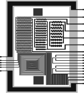
Figure 2. Mask diagram including
the three required layers to process the microchip. The two red-square regions
have a side length of 900 (top) and 1000 (bottom) mm and serve to build the
inlet and outlet holes by micromachining. The green rectangle of 800 mm in
width will be used to pattern the photoresin. The blue level contains diverse
electrode microarrays and will outline the metal layer
The metal layer is organized into three main regions including microelectrodes for c-DEP, ROT and TWD phenomena. The first array is composed by classical and shifted interdigitated castellated electrodes, as well as saw-teeth electrodes that can be employed in c-DEP studies. The second region corresponds to a square spiral microarray shaped by four wound planar electrodes, which is intended for TWD-based particle microhandling. The last structure consists of two quadrupolar microelectrodes of square and triangular shapes which were patterned to perform ROT srudies. Furthermore a meandering wire was included in order to form a resistor to sense thermal changes inside the suspending medium.
The resin level contains a rectangular frame of 800 mm width to mould the microchamber walls. This value is a technological requirement of the casting procedure, which also constrains the minimum distance between the outer edge of the wall and the electrode pads. Leaving enough space for the wire bonding by thermocompression, as well as process tolerances must be kept in mind. In this case such a distance was 630 mm.
2.3 Fabrication process
The technological process at the wafer level can
be divided into three stages. The first one is the microelectrode patterning
in which metal electrodes are defined onto a silicon wafer of 300 mm thickness
by means of two techniques: photolithography to pattern gold electrodes, and
lift-off to pattern platinum electrodes. After that, the wafer is drilled by
silicon micromachining in order to shape the inlet and outlet holes. The wafer-level
processing ends up with the photolithographic structuring of an UV-curable
polymer to cast the microchamber walls.
Figure 3 depicts the most relevant technological steps followed to fabricate the dielectrophoretic-based microsystem at the wafer level. In the sequel a brief summary of the fabrication process is produced.
- The starting material was a p-doped silicon wafer, doped with boron till a resistivity of 4 40 W cm-1, of 300 mm thickness (1).
- Once wafers have been cleaned, oxidation is produced yielding SiO2 layers of 8000 Å thickness (2).
- After that, a silicon nitride (Si3N4) layer of 1800 Å is deposited by PECVD onto the backside of the wafer (3).
- Then, photolithography onto the component side is done employing the metal level mask, to pattern gold microelectrodes of 500 Å thickness onto a titanium layer of 1000 Å (4-5).
- Also, a lift-off process is carried out to pattern platinum microelectrodes of 1500 Å thickness onto a titanium layer of 500 Å (4’- 5’).
- Etching of both Si3N4 and SiO2 layers on the backside of the wafer, employing the micromachining level mask (6).
- Anisotropic etching of the silicon substrate (300 mm) by TMAH (tetramethylammonium hydroxide) till the silicon oxide field (7).
- Etching of the SiO2 field membrane using a solution of SiO-ETC, to finish the micromachining of inlet and outlet holes (8).
- UV-curing of polydimethylsiloxane (PDMS) onto the component side to cast the microchamber walls (9).
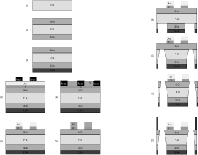
Figure 3. Schematic
flow diagram of the fabrication process employed to develop the microsystem.
Steps 1 to 3 are shared by wafers with gold and platinum electrodes. Steps
4 and 5 represent the gold electrode deposition by common photolithography
while steps 4’ and
5’ illustrate the lift-off technique to pattern the platinum electrodes. Steps
6 to 9 are also shared and represent the silicon micromachining and micropool
wall casting
3. RESULTS AND DISCUSSION
3.1 Microelectrode
description
As previously described, there are microelectrodes
of gold and platinum developed by photolithography and lift-off processes,
respectively. The utilization of these two metals will be advantageous in order
to compare their performance with respect to biocompatibility when working
with bioparticles.
The metal layer can be divided into three main regions including microelectrodes for c-DEP, ROT and TWD phenomena. The first array is actually composed by three microstructures (see figure 4), each one formed by classical and shifted interdigitated castellated electrodes, as well as saw-teeth electrodes with typical sizes of 50, 70 and 90 mm in both electrode length and separation. Figures 5 and 6 show detailed views of interdigitated castellated and saw-teeth microelectrodes. In order to gain flexibility, electrodes of different size have their own pads to be externally accessed. These microelectrodes can be employed in c-DEP studies and separation of microparticles ranging from 4 mm to 30 mm depending on the selected array. It can be pointed out that dimensions could be scaled down to allow the study of smaller particles than those previously mentioned, but it was not the purpose of this work.
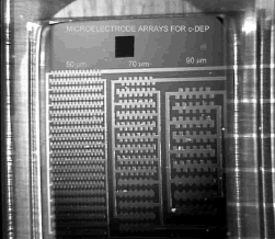
Figure 4. Platinum microstructures
containing classical and shifted interdigitated castellated, as well as saw-teeth
microelectrodes

Figure 5. Photographs of classical
and shifted Interdigitated castellated microelectrodes of 50, 70 and 90 mm
in typical dimension (from left to right)

Figure 6. Photographs of saw-teeth
microelectrodes of 90 and 70 mm, and a detail of microelectrodes of 50 mm in
typical dimension (from left to right)
The second region of the metal layer corresponds to a square spiral microarray shaped by four wound planar electrodes of 20 mm in width and 28 mm in the interelectrodic gap (see figure 7), which is intended for TWD-based particle micromotion.
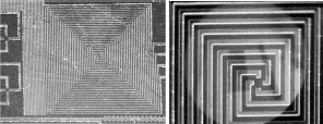
Figure 7. Total view of the
square spiral microarray with a side length of 2700 mm (left), and partial
view of the central part of the same platinum spiral (right)
The last structure consists of two quadrupolar microelectrodes of square and triangular shapes as shown in figure 8, which were patterned to assay particles by means of the electrorotation technique.

Figure 8. Quadrupoles of 50
mm in electrode width and 100 mm in separation. On the left a total view of
both microstructures is shown, while the other two photographs reproduce a
detailed view of the square and triangular microelectrodes
Additionally, a meandering wire of 20 mm in width and 113 mm in length was included in order to form a resistor to sense thermal changes inside the suspending medium (see figure 9). Such a resistor could be utilized in long-term experiments with cell cultures under the influence of high-strength electric fields, to determine and correlate the temperature changes with possible variations in the cell physiology. It can be also used to establish if further convection around the chip is required when DEP experiments are in progress. The real value of the wire resistor, R, is giving as:
![]()
where l stands for the wire length, w for its width and Rsq for the square resistance (expressed in W per square). In this case, there were two parallel runs made of platinum (measured Rsq = 1.22) and gold (measured Rsq = 1.45), which yielded resistors of 6895 and 8195 W, respectively.
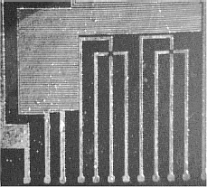
Figure 9. View
of the platinum meandering wire. The assessed resistor value was 6895 W while
its measured value was 6800 W at 25 °C
3.2 Silicon micromachining
This well-known technology allows the micromechanization of three-dimensional silicon structures with a high degree of precision. As wafers of 300 mm had to be completely drilled to shape the inlet and outlet ports, bulk micromachining or anisotropic wet etching of silicon wafers by means of alkaline solutions was employed (see figure 10).
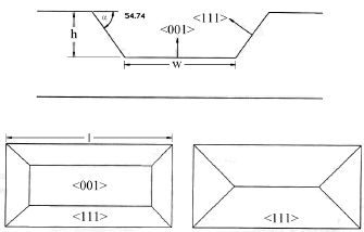
Figure 10. Cross
section and top views of rectangular windows anisotropically etched on a
silicon wafer aligned to direction
<110>. If the window length, l, is small and the wafer thickness
is big enough, the etching progress ends up when the four planes <111> intersect
among them (rectangle on the right). However, under the adequate relationship
between window area and wafer thickness, a square or rectangular hole can be
drilled. (rectangle on the left) [50]
After a brief straightforward geometrical manipulation, the final side width of the micromachined hole (w) can be obtained as:
![]()
where l is the side length of the square used as mask on the backside of the wafer, h is the hole depth, and a = 54.74° as depicted in figure 10.
In this case, l was constrained by the external diameter (1/32” = 793 mm) of the Teflon capillary tube which will be glued to the micromachined hole in order to shape the inlet and outlet ports of the suspending medium. Two different lengths were chosen for each hole in order to facilitate the particle circulation around the microchamber: li = 900 mm (inlet) and lo = 1000 mm (outlet), respectively.
As the wafer thickness was 300 mm, the final size of such holes were wi = 476 mm and wo = 576 mm, respectively. Figure 11 shows the result of the silicon micromachining process carried out by technological steps 6 to 8 described in figure 3.
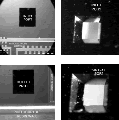
Figure 11. Front side (left)
and backside (right) of the silicon substrate after anisotropic etching by
means of TMAH
3.3 Micropool casting
The proposed procedure is based on the use of a
photopatternable silicone deposited on the whole silicon wafer containing microelectrode
arrays. The first step of this process consists of designing a mask with the
pattern to be transferred to the silicon layer. This mask should leave the
active microelectrode area as well as the bonding pads free from silicone,
so that the electrodes have not additional coating that could influence the
induction of electric field inhomogeneities, reducing its performance.
The micropool casting process is composed by the following steps: i) deposition of the silicone layer over the whole wafer up to the desired thickness, ii) mask alignment, iii) UV exposure of the resin, iv) removal of the non-cured silicone, followed by v) rinse in de-ionized water and dry.
The photopatternable material was a UV-curable photo-negative silicone called polydimethylsiloxane (PDMS) SemicosilÒ 948 UV supplied by Wacker Chemie. Despite this resin has adhesive characteristics to silicon substrates and prior treatment of the wafer surface is not necessary, before PDMS deposition the surface was treated with a solution of MPTS in methanol (10% 3-metacrylooxypropyltrimetoxy-silane, 90% methanol) in order to improve the resin adhesion[51].
The thickness of the polymer layer is around 1 mm and curing was done in 50 sec with a conventional mask aligner. After exposure to UV light only rectangular patterns are cross-linked. The nonexposed areas of PDMS are removed in the developing step, which consists of soaking the wafer in n-hexane or xylene, followed by isopropanol and finally a rinse of de-ionized water. The final result is a rectangular UV-molded silicone elastomer frame, i.e. the micropool walls of 800 mm in width as shown in figure 12, around the electrode active area. Such a frame has internal length and width of 9598 and 5480 mm, respectively, limiting an area of 52.6 mm2 which finally yields a total enclosed volume of 52.6 mm3.
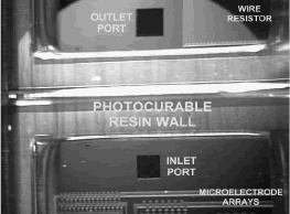
Figure 12. Partial view of the
photosensitive resin walls of two adjacent chips before of being diced. Inlet
and outlet ports can also be seen
The main advantage of this process is that photoresin has excellent adhesion to the silicon surface and the deposited walls perfectly adapt themselves to the wafer surface irregularities (including the electrode wires) as can be seen in figure 13, which avoids tedious, time-consuming and costly design efforts to connect the inner electrodes to the outer pads. As a result of this process, a micropool of known volume is formed allowing the use of the same sample volume during all the experimental stage.
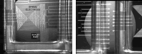
Figure
13. Photographs of the spiral and quadrupolar microelectrode arrays
(left) and a detail of their pads (right) before dicing. Photoresin transparent
walls can be clearly observed, as well as electrode wires crossing under
them to connect the electrodes themselves to the external pads
This process has an enormous potential in the field of microsystems. In our case, the automatic deposition of walls at the wafer level enhances the advantages of batch processing initially restricted to the planar silicon technique. In other words, such a process eliminates the need for a one-by-one wall casting and simplifies the fabrication process considerably.
3.4 The final microsystem
At this point of the fabrication process, the wafer is ready to be diced. Each die will be glued onto a PCB (Print Circuit Board) especially designed to this purpose. Such a PCB will be conveniently drilled to allow the assembly of the fluidic interface (TeflonÒ tubes appropriately attached to the micromachined holes). Lastly, wire bonding will be produced in order to complete the electrical interface.
Figure 14 shows a photograph of a microsystem for bioparticle microhandling assembled as described in the preceding paragraph, remaining only the wire-bonding step to be performed.
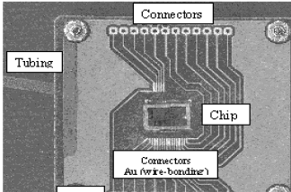
Figure
14. Photograph of the microsystem mounted on a PCB (5.5 cm in width
and length) with wire-tracks metallised of gold to facilitate the chip
wire-bonding procedure. Plastic tubing conveniently glued to the backside
of the microstructure can be easily seen
4. CONCLUSIONS
The microdevice presented here was conceived to explore the possibilities of microsystems addressed to bioparticle handling based on the diverse dielectrophoretic effects. To attain this goal, activities were orientated towards the design and fabrication of microstructures which adapt themselves to the electrohandling of microparticles both artificial and natural.
It must be stressed that by using microelectrode structures, various forms of electric fields, such as non-uniform, rotating and travelling wave, can be imposed on particles of sizes ranging from proteins and viruses to micro-organisms and cells. Each type of particle responds to the forces exerted on them in a unique way, allowing for their controlled and selective manipulation as well as their characterization.
Since a technological point of view, standard CMOS technology could be used to develop microtools addressed to microparticle handling. The main advantage of devices manufactured in this technology is that active control circuitry required to develop a true microsystem-on-a-chip structure may be integrated onto them. However, when working in bioparticle microhandling, one must be aware of the biocompatibility problems likely originated by liberation of aluminum ions in the suspending medium. In other words, if biocompatibility is a strong restriction, electrodes made of noble metals should be used.
In view of this, a whole microsystem was designed and fabricated by means of microfabrication techniques. This microsystem hinges on the various dielectrophoretic phenomena (c-DEP, ROT and TWD) and may be employed to perform diverse bioelectronic experiments such as characterization, separation and motion of microparticles, and culture of micro-organisms under the influence of strong electric fields. Such a microstructure includes a silicon substrate onto which electrodes of gold and platinum were grown by photolithography and lift-off techniques. Moreover, the substrate was drilled to shape the inlet and outlet fluid ports employing bulk silicon micromachining techniques. Holes patterned by such a technique will serve to bring the suspending medium onto the electrode surface and once the desired measurements have been done, carry away the mixture to further analysis if necessary.
Microcavity walls were molded by means of a photopatternable resin (PDMS). As a result of this process, a micropool of known volume is formed allowing the use of the same sample volume during all the experimental stage. The main advantage of the photocured technique is that photoresin has excellent adhesion to the silicon surface and the deposited walls perfectly adapt themselves to the wafer surface irregularities (including the electrode wires), which avoids tedious, time-consuming and costly design efforts to connect the inner electrodes to the outer pads.
To conclude, it must be stressed that microsystem-related technologies employed here, i.e. photolithography, silicon micromachining and polymer deposition, have a brilliant future when designing and fabricating microdevices addressed to bioparticle microhandling hinging upon dielectrophoretic phenomena. Some reasons for this are that microsystems can be manufactured with dimensions adequate to those required by microparticle manipulation, and that the required components like electrical, fluidic, and optical interfaces can be easily integrated.
5. ACKNOWLEDGEMENTS
The authors are grateful to the Microelectronics National Center (CNM) in Barcelona, Spain , and especially to Dr. Errachid Abdelhamid, for manufacturing and processing the microchip described here.
REFERENCES
[1] RUIZ, O., RUBIO, C., MARCO, S., CARMONA, M., SAMITIER, J., MORANTE J. Optimization of voltage-controlled thin-film microstructures. Sensors and Actuators A, Vol. 46-47. 1995. pp. 613-617.
[2] MARCO, S., SAMITIER, J., RUIZ, O., MORANTE, J., ESTEVE, J. High-performance
piezoresistive pressure sensors for biomedical applications using very thin
structures membranes. Measurement Science and Technology, Vol. 7. 1996. pp.
11951203.
[3] CARMONA, M., MARCO, S., SAMITIER, J., MORANTE, J. Dynamic simulation of micropumps. Journal of Micromechanics and Microengineering, Vol. 6. 1996. pp. 128-130.
[4] CARMONA, M., S. MARCO, J. SAMITIER, M. ACERO, J. PLAZA & J. ESTEVE.
Modelling of silicon passive microvalves. The 13th European Conference on Solid-State
Transducers EUROSENSORS XIII. The Hague, The Netherlands . 721 - 724. September
12-15, 1999.
[5] EATON, W., SMITH, j. Micromachined pressure sensors: review and recent developments. Smart Mater. Struct. Vol. 6. 1997. pp. 530 - 539.
[6] HOUMMADI, L., CAMPITELLI, A., WLODARSKI, W. Acoustic wave sensors: design, sensing mechanisms and applications. Smart Mater. Struct. Vol. 6. 1997. pp. 647 - 657.
[7] LEE, C., LIN, Y-S. A new mechanism for transformation of small displacements
to large rotations for a VOA. IEEE Sensors Journal, Vol. 4. 2004. pp. 503509.
[8] KIM J., VARADAN, V., BAO, X. Finite element modeling of a smart cantilever plate and comparison with experiments. Smart Mater. Struct. Vol. 5. 1996. pp. 165 - 170.
[9] REBELLO, K. Applications of MEMS in surgery. Proceedings of the
IEEE. Vol. 92. 2004. pp 43 55.
[10] FUHR, G., SHIRLEY, S. G. Biological application of microstructures. Topics in current chemistry, Vol. 194. 1998. pp. 83-116.
[11] AHN, C., J. CHOI, G. BEAUCAGE, J. NEVIN, J. LEE, A. PUNTAMBEKAR,
J. LEE. Disposable smart lab-on-a-chip for point-of-care clinical diagnostics.
Proceedings of the IEEE Vol. 92. 2004. pp 154 163.
[12] FUHR, G., T. MÜLLER, T. SCHNELLE, R. HAGEDORN, A. VOIGT, S. FIEDLER.
Radio-frequency microtools for particle and living cell manipulation. En :
Naturwissenschaften Vol. 81. 1994. pp. 528 - 535.
[13] REED, M.,W. LYE. Microsystems for drug and gene delivery. Proceedings
of the IEEE Vol. 92. 2004. pp. 56 75.
[14] PORRAS, Y. M., PEDRAZA, O. A., FERNÁNDEZ, F. H., DUARTE, J. E. Manipulación de protozoos por ultrasonido. Revista Colombiana de Biotecnología. Vol. VI No. 1. 2004. pp. 79 84.
[15] MÜLLER, T., PFENNIG, A., KLEIN, P., GRADL, G., JÄGER, M., SCHNELLE, T. The potential of dielectrophoresis for single-cell experiments. IEEE in Medicine and Biology Magazine, Vol. 22. 2003. pp. 5161.
[16] GASCOYNE, P., J. VIKOUKAL. Dielectrophoresis-based sample handling
in general-purpose programmable diagnostics instruments. Proceedings of the
IEEE Vol. 92. 22 42. 2004.
[17] HAGA, Y., M. ESASHI. Biomedical microsystems for minimally invasive
diagnosis and treatment. Proceedings of the IEEE. Vol. 92. 98 114. 2004.
[18] HOLMES, D., GREEN, N., MORGAN, H. Microdevices for dielectrophoretic flow- through cell separation. IEEE in Medicine and Biology Magazine Vol. 22. 2003. pp. 85 - 90.
[19] MÜLLER, T. A., GERARDINO, T., SCHNELLE, S., SHIRLEY, F., BORDONI,
G., DE GASPERIS, R., FUHR, G. Trapping of micrometre and sub-micrometre particles
by high-frequency electric fields and hydrodinamic forces. J. Phys. D: Appl.
Phys. Vol. 29. 1996. pp. 340 - 349.
[20] HUGHES, M. P., MORGAN, H., RIXON, F., BURT, J., PETHIG, R. Manipulation of herpes simplex virus type 1 by dielectrophoresis. Biochimica et Biophysica Acta, Vol. 1425. 1998. pp. 119-126.
[21] ASBURY, C. L., VAN DEN ENGH, G. Trapping of DNA in nonuniform oscillating electric fields. Biophysical Journal, Vol. 74. 1998. pp. 1024-1030.
[22] POHL, H. A. The motion and precipitation of suspendoids in divergent electric fields. J. of Appl. Phys. Vol. 22. 1951. pp. 869 - 871.
[23] POHL H, A. Some effects of nonuniform fields on dielectrics. En : J. Appl. Phys. Vol. 29. 1958. pp. 1182 - 1188.
[24] POHL, H. A., PETHIG, R. Dielectric measurements using non-uniform electric field (dielectrophoretic) effects. Journal of Physsics E: Scientific Instruments, Vol. 10. 1977. pp. 190-193. Corrigendum 883.
[25] GREEN, N.G., MORGAN, H. Dielectrophoresis of submicrometer latex spheres. 1. Experimental results. Journal of Physical Chemistry B, Vol. 103. 1999. pp. 41-50.
[26] HAWKES, J., ARCHER, G., BETTS, W. A dielectrophoretic spectrometer
for characterising micro-organisms and other particles. Microbios, Vol. 73.
1993. pp. 8186.
[27] QUINN, C., ARCHER, G., BETTS, W., O'NEILL, J. Dose-dependent dielectrophoretic response of Cryptosporodium oocysts treated whit ozone. Letters in Applied Microbiology Vol. 22. 1996. pp. 224 - 228.
[28] SCHNELLE T., HAGEDORN, R., FUHR, G., FIEDLER, S., MÜLLER, T. Three-dimensional
electric field traps for manipulation of cells - calculation and experimental
verification. Biochimica et Biophysica Acta, Vol. 1157. 1993. pp. 127 - 140.
[29] PETHIG, R., HUANG, Y., WANG, X-B., BURT, J. P. Positive and negative dielectrophoretic collection of colloidal particles using interdigitated castellated microelectrodes. J. Phys. D: Appl. Phys. Vol. 24. 1992. pp. 881 - 888.
[30] WANG, X-B., HUANG, Y., HÖTZEL, R., BURT, J. P., PETHIG, R. Theoretical
and experimental investigations if the interdependence of the dielectric, dielectrophoretic
and electrorotational behaviour of colloidal particles. J. Phys. D: Appl. Phys.
Vol. 26. 1993. pp. 312 - 322.
[31] ZHOU, H.,BURT, J., PETHIG, R. Automatic cell electrorotation measurements:
studies of the biological effects of low-frequency magnetic fields and of heat
shock. Physics in Medicine and Biology, vol. 43. 1998. pp. 1075 1090.
[32] NISHIOKA, M., KATSURA, S., HIRANO, K., MIZUNO, A. Evaluations of cell characteristics by step-wise orientational rotation using optoelectrostatic micromanipulation. IEEE Trans. on Ind. Appl. Vol. 33. 1997. pp. 1381 - 1388.
[33] HUGHES, M. P., WANG, X-B., BECKER, F. F., GASCOYNE, P. R., PETHIG, R. Computer-aided analyses of electric fields used in electrorotation studies. J. Phys. D: Appl. Phys. Vol. 27. 1994. pp. 1564 - 1570.
[34] ARNOLD, W. M., SCHWAN, H. P., ZIMMERMANN, U. Surface conductance and other properties of latex particles measured by electrorotation. J. Phys. Chem. Vol. 91. 1987. pp. 5093 - 5098.
[35] GRIFFITH, A., COOPER, J. Single-cell measurements of human neutrophil
activation using electrorotation. Anal. Chem. Vol. 70. 1998. pp. 2607 2612.
[36] HUGHES, M.P., PETHIG, R., WANG, X-B. Dielectrophoretic forces on particles in travelling electric fields. Journal of Physics D: Applied Physics, Vol. 29. 1996. pp. 474-482.
[37] PETHIG, R., M. TALARY, R. LEE. Enhancing traveling-wave dielectrophoresis with signal superposition. IEEE in Medicine and Biology Magazine Vol. 22. 2003. pp. 43 - 50.
[38] MASUDA, S., WASHIZU, M., IWARADE, M. Separation of small particles suspended in liquid by nonuniform travelling field. IEEE Transactions on Industry Applications, Vol. IA-23, No. 3. 1987. pp. 474-480.
[39] GOATER, A., BURT, J.P.H., PETHIG, R. A combinated travelling wave dielectrophoresis and electrorotation device: applied to the concentration and viability determination of Cryptosporidium. Journal of Physics D: Applied Physics, Vol. 30. 1997. pp. L65-L69.
[40] HUANG, Y., WANG, X-B., TAME, J., PETHIG, R. Electrokinetic behaviour of colloidal particles in travelling electric fields: studies using yeast cells. Journal of Physics D: Applied Physics, Vol. 26. 1993. pp. 1528-1535.
[41] FERNÁNDEZ, F., SAMITIER, J. CMOS spiral microstructure for TWD applications. In: Fifth Conference of the European Society for Engineering and Medicine, ESEM’99, Barcelona, Spain, p. 177178,
30 May to 2 June 1999.
[42] WISE K., D. ANDERSON, J. HETKE, D. KIPKE, K. NAJAFI. Wireless implantable
Microsystems: high-density electronic interfaces to the nervous system. Proceedings
of the IEEE Vol. 92. 76 97. 2004.
[43] SUEHIRO, J., PETHIG, R. The dielectrophoretic movement and positioning of a biological cell using a three-dimensional grid electrode system. Journal of Physics D: Applied Physics, Vol. 31. 1998. pp. 3298-3305.
[44] PAUL, C., HARRISON, J. Transport, manipulation and reaction of
biological cells on-chip using electrokinetic effects. Analytical Chemistry,
Vol. 69. 1997. pp. 15641568.
[45] PETHIG, R., BURT, J. P., PARTON, A., RIZVI, N., TALARY, M. S., TAME, J. A. Development of biofactory-on-a-chip technology using excimer laser micromachining. Journal of Micromechanics and Microengineering, Vol. 14. 1998. pp. 57-63.
[46] BURT, J. P., AL-AMEEN, T. A. K., PETHIG, R. An optical dielectrophoresis spectrometer for low-frequency measurements on colloidal suspensions. Journal of Physics E: Scientific Instruments, Vol. 22. 1989. pp. 952-957.
[47] CLERC, P., DELLMANN, L., GRÉTILLAT, F., GRÉTILLAT, M., INDERMÜHLE, P., JEANNERET, S., LUGINBUHL, P. H., MARXER, C., PFEFFER, T., RACINE, G., ROTH, S., STAUFER, U., STEBLER, C., THIÉBAUD, P., DE ROOIJ, N. Advanced deep reactive ion etching: a versatile tool for microelectromechanical systems. Journal of Micromechanics and Microengineering, Vol. 8. 1998. pp. 272 278.
[48] FUHR, G., FIEDLER, S., MÜLLER, T., SCHNELLE, T., GLASSER, H. Particle
micromanipulator consisting of two orthogonal channels with travelling-wave
electrode structures. Sensors and Actuators A, Vol. 41-42. 1994. pp. 230-239.
[49] KRASSOW, H., F. CAMPBADAL, E. LORA-TAMAYO. Wafer level packaging
of silicon pressure sensors. In: TRANSDUCERS'99, Sendai, Japan , p. 11481151,
7-10 June 1999.
[50] MARCO, S. Optimización de sensores de presión piezorresistivos de silicio para instrumentación biomédica
y aplicaciones a alta temperatura. [PhD Thesis]. Dissertation, University of
Barcelona, Barcelona, Spain , p. 130. 1993.
[51] RASSOW, H. Microsensor packaging for flow measurement with a novel
differential pressure meter. [PhD Thesis]. Dissertation, Universitat Autònoma
de Barcelona, Barcelona, Spain, p153,1999.
Cómo citar
IEEE
ACM
ACS
APA
ABNT
Chicago
Harvard
MLA
Turabian
Vancouver
Descargar cita
Visitas a la página del resumen del artículo
Descargas
Licencia
Derechos de autor 2008 DYNA

Esta obra está bajo una licencia internacional Creative Commons Atribución-NoComercial-SinDerivadas 4.0.
El autor o autores de un artículo aceptado para publicación en cualquiera de las revistas editadas por la facultad de Minas cederán la totalidad de los derechos patrimoniales a la Universidad Nacional de Colombia de manera gratuita, dentro de los cuáles se incluyen: el derecho a editar, publicar, reproducir y distribuir tanto en medios impresos como digitales, además de incluir en artículo en índices internacionales y/o bases de datos, de igual manera, se faculta a la editorial para utilizar las imágenes, tablas y/o cualquier material gráfico presentado en el artículo para el diseño de carátulas o posters de la misma revista.


