Published
CARACTERIZACIÓN OPTO-ELÉCTRICA DE BICAPAS n+-ZnO/i-ZnO CRECIDAS IN SITU POR EVAPORACIÓN REACTIVA SIN USAR DOPAJE EXTRÍNSECO
OPTO-ELECTRICAL CHARACTERIZATION OF n+-ZnO/i-ZnO BILAYERS GROWN IN SITU BY REACTIVE EVAPORATION WITHOUT USING EXTRINSIC DOPING
DOI:
https://doi.org/10.15446/mo.n52.58890Keywords:
Películas delgadas de ZnO, evaporación reactiva, propiedades opto-eléctricas, instrumentación virtual, dopaje intrínseco. (es)ZnO thin films, reactive evaporation, opto-electrical properties, virtual instrumentation, intrinsic doping. (en)
Downloads
Este trabajo describe un procedimiento para crecer in situ películas delgadas de n+-ZnO e i-ZnO altamente transparentes, depositadas secuencialmente por evaporación reactiva asistido por plasma sin usar dopaje extrínseco. Se logró una buena reproducibilidad del espesor y de las propiedades opto-eléctricas de las películas a través de un control electrónico novedoso desarrollado usando el concepto de instrumentación virtual. Para lo cual se implementó un instrumento virtual (VI) que controlaba el proceso usando PID (proportional integral differential) y PWM (pulse width modulation) como algoritmos de control. Optimizando el diseño del reactor y los parámetros de deposición se obtuvieron con este método películas n+-ZnO e i-ZnO con resistividades alrededor de 6 x 10⁻⁴ cm y 104 cm respectivamente y transmitancias mayores al 85% (en la región visible). A partir de medidas de energía Urbach encontramos que las películas n+-ZnO depositadas controlando apropiadamente la cantidad de zinc que llega al reactor tienen una cantidad baja de defectos estructurales. También se reportan resultados relacionados con propiedades de transporte eléctrico de las películas de ZnO, obtenidas de medidas de conductividad y movilidad dependientes de la temperatura.
This work describes a procedure to grow in situ highly transparent n+-ZnO and i-ZnO thin films sequentially deposited by plasma assisted reactive evaporation without using extrinsic doping. Good reproducibility of the thickness and opto-electrical properties of the films was achieved through a novel electronic control developed using the virtual instrumentation concept. For that, a virtual instrument (VI) was implemented to control the process using PID (proportional integral differential) and PWM (pulse width modulation) as control algorithms.
By optimizing the design of the reactor and deposition parameters, n+-ZnO and i-ZnO films with resistivities around 6 x10⁻⁴ cm and 104 cm respectively and transmittances greater than 85% (in the visible region) were obtained with this method. From Urbach energy measures we have found that n+-ZnO films deposited controlling the quantity of zinc that arrives to the reactor appropriately, have a low density of structural defects. Results regarding electrical transport properties of the ZnO films, obtained from temperature dependent measurements of both conductivity and mobility, are also reported.
OPTO-ELECTRICAL CHARACTERIZATION OF n+-ZnO/i-ZnO BILAYERS GROWN IN SITU BY REACTIVE EVAPORATION WITHOUT USING EXTRINSIC DOPING
CARACTERIZACIÓN OPTO-ELÉCTRICA DE BICAPAS n+-ZnO/i-ZnO CRECIDAS IN SITU POR EVAPORACIÓN REACTIVA SIN USAR DOPAJE EXTRÍNSECO
Asdrúbal A. Ramírez1, Johana S. Oyola2, Clara L. Calderón2, Gerardo Gordillo2
1 Grupo de Materiales Semiconductores y Energía Solar, Facultad de Ingeniería, Universidad Nacional de Colombia - Bogotá, Colombia
2 Grupo de Materiales Semiconductores y Energía Solar, Facultad de Ciencias, Departamento de Física, Universidad Nacional de Colombia - Bogotá, Colombia
Clara L. Calderón: clcalderont@unal.edu.co
(Recibido: Noviembre/2015. Aceptado: Abril/2016)
Abstract
This work describes a procedure to grow in situ highly transparent n+-ZnO and i-ZnO thin films sequentially deposited by plasma assisted reactive evaporation without using extrinsic doping. Good reproducibility of the thickness and opto-electrical properties of the films was achieved through a novel electronic control developed using the virtual instrumentation concept. For that, a virtual instrument (VI) was implemented to control the process using PID (proportional integral differential) and PWM (pulse width modulation) as control algorithms. By optimizing the design of the reactor and deposition parameters, n+-ZnO and i-ZnO films with resistivities around 6 x 10⁻⁴ Ωcm and 104 Ωcm respectively and transmittances greater than 85 % (in the visible region) were obtained with this method. From Urbach energy measures we have found that n+-ZnO films deposited controlling the quantity of zinc that arrives to the reactor appropriately, have a low density of structural defects. Results regarding electrical transport properties of the ZnO films, obtained from temperature dependent measurements of both conductivity and mobility, are also reported.
Keywords: ZnO thin films, reactive evaporation, opto-electrical properties, virtual instrumentation, intrinsic doping.
Resumen
Este trabajo describe un procedimiento para crecer in situ películas delgadas de n+-ZnO e i-ZnO altamente transparentes, depositadas secuencialmente por evaporación reactiva asistido por plasma sin usar dopaje extrínseco. Se logró una buena reproducibilidad del espesor y de las propiedades opto-eléctricas de las películas a través de un control electrónico novedoso desarrollado usando el concepto de instrumentación virtual. Para lo cual se implementó un instrumento virtual (VI) que controlaba el proceso usando PID (proporcional integral differential) y PWM (pulse width modulation) como algoritmos de control. Optimizando el diseño del reactor y los parámetros de deposición se obtuvieron con este método películas n+-ZnO e i-ZnO con resistividades alrededor de 6 x 10⁻⁴ Ωcm y 104 Ωcm respectivamente y transmitancias mayores al 85% (en la región visible). A partir de medidas de energía Urbach encontramos que las películas n+-ZnO depositadas controlando apropiadamente la cantidad de zinc que llega al reactor tienen una cantidad baja de defectos estructurales. También se reportan resultados relacionados con propiedades de transporte eléctrico de las películas de ZnO, obtenidas de medidas de conductividad y movilidad dependientes de la temperatura.
Palabras clave: Películas delgadas de ZnO, evaporación reactiva, propiedades opto-eléctricas, instrumentación virtual, dopaje intrínseco.
1. Introduction
ZnO thin films have been extensively studied for use as transparent and conductive window layers in chalcopyrite and kesterite based solar cells [1-3]. Recently this compound also began to be used as electron selective layer in inverted organic solar cells [4, 5] and as electron transport layer in perovskite based hybrid solar cells [6, 7]. Various methods, such as: rf magnetron sputtering [8], reactive sputtering [9], chemical vapor deposition (CVD) [10], chemical bath deposition (CBD) [11], spray pyrolysis [12] and sol gel techniques [13], have been used to fabricate ZnO films. Among these methods, magnetron rf sputtering is considered the most favorable technique for large area deposition and mass production. High CIGS solar cell efficiencies up to 20.5% have been achieved for RF-sputtered ZnO:Al films from ceramic targets [14]. However, the rf sputtering deposition process has cost limitations in large-area manufacturing, associated with the use of ceramic targets. In contrast, ZnO deposited by reactive evaporation with Zn as the starting material, is in terms of cost and large scale production better than the rf sputtering technique; however, the main advantages of this method are: (a) polycrystalline material is directly obtained during the deposition process without the need for further heat treatment and (b) the resistivity of the ZnO thin films can be varied in a wide range (10-4 to 104 Ωcm) without using extrinsic doping; the strong variation of resistivity can be achieved through generation of oxygen vacancies (intrinsic doping). Various routes have been used to grow polycrystalline and nanostructured ZnO thin films by activated reactive evaporation. ZnO films with polycrystalline wurtzite structure have been grown following a route consisting of the evaporation of Zn metal from a molybdenum boat in presence of oxygen gas ionized with a cold cathode ion source [15] and ZnO nanoneedles have also been synthesized by thermally evaporating pure Zn at a high rate through oxygen plasma [16].
In this paper we describe a novel procedure developed to grow ZnO thin films by the plasma assisted reactive evaporation method. The innovative aspect includes both the design of the reactor used for the sequential deposition of thin films of i-ZnO and n+-ZnO in situ and an electronic system developed using virtual instrumentation [17]. The system allows to control in a reproducible way the growth of i-ZnO and n+-ZnO films with opto-electrical properties suitable for their use as window layers in solar cells. This was achieved through a virtual instrument with facilities to control with good precision the flow of evaporated Zn that is the parameter most critically affecting both the reproducibility and the opto-electrical properties of ZnO. The main characteristic of the developed VI, is that it includes PID and PWM algorithms to perform the control of the process using a K-type thermocouple as temperature sensor for the Knudsen cell used as Zn evaporation source, and a pirani gauge as sensor for the change of partial pressure inside the chamber (that occurs when evaporated Zn starts its reaction with the oxygen present in the chamber). Results from characterization of the ZnO thin films obtained through measurements of spectrophotometry, temperature dependent conductivity, Hall mobility and Urbach energy are also reported.
2. Experimental
The ZnO thin films were deposited at room temperature on soda-lime glass substrates using a route based on the plasma assisted reactive evaporation method, which consists of evaporating Zn in the presence of oxygen so that a chemical reaction takes place giving rise to the formation of the ZnO. As the Zn in the presence of O2 oxidize very slowly at room temperature, it is necessary to ionize both the Zn and the O2 to accelerate the chemical reaction between these two species. The ionization is achieved through a glow discharge (GD); the generated plasma includes different ionized species that increase the speed of the chemical reaction and therefore the rate of ZnO film growth.
As under the conditions of current and pressure used in the reactive evaporation process, the generated plasma is a non-thermal plasma, therefore the most probable mechanism of gas ionization inside the plasma is direct ionization of neutral particles (atoms, molecules or radical) by electron impact [18, 19].
The potential difference applied between the electrodes to generate the glow discharge induces the following processes:
I) Dissociation of O2 followed by the release of sufficient energy to ionize the atoms of oxygen present. In the first moments are generated the following species:
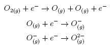
II) When Zn vapor enters the region of glow discharge the following species of zinc positively ionized can be generated:

III) Once the precursor species (O and Zn) are ionized, they can be neutralized by binary collisions through the process of recombination and removal of ions:

IV) Finally, the ZnO(g) generated in the plasma is diffused toward the substrate to form the thin film; during this process the ZnO(g) can interact with the plasma and can also be ionized:

This type of reactions allows the plasma to remain stable. To design the reactor that allows generating a stable glow discharge confined in the space between the electrodes, the Paschen law, that relates the voltage for the initiation of the discharge and the product of the pressure by the separation distance between the electrodes, was taken into account [19]. Under the conditions of oxygen partial pressure used (2.5 - 4 x 10⁻² mbar), the reactor designed allows obtaining a stable glow discharge applying a voltage difference around of 500 V. The system used to grow ZnO thin films by plasma assisted reactive evaporation method includes the following units:
a) Deposition chamber connected to a vacuum system, consisting of a mechanical pump and a trap of liquid nitrogen that allows getting a base pressure of 10-4 mbar, prior to the introduction of oxygen. Inside the chamber the rector was installed in which takes place the chemical reaction of precursors (O2 and Zn) giving rise to the formation of the ZnO and the source of evaporation of zinc (Knudsen cell), whose temperature is automatically controlled with a PID control (proportional, integral, differential). The reactor includes parallel flat electrodes supported by a structure of Teflon, which are connected to an external DC power supply (2000 V, 200 mA) regulated at both voltage and current, to activate the GD.
b) Electronic mass flow controller which allows precisely controlling the flow of oxygen introduced to the chamber.
c) Control unit, whose main function is to control, with very good precision, the amount of zinc that arrives to the GD zone, which is provided by the evaporation from the Knudsen cell.
The obtaining of conditions to deposit in situ and in reproducibly way the bilayer i-ZnO/n+-ZnO with thicknesses, transmittances and resistivities suitable for their use as optical windows in solar cells, is very difficult due to the fact that, in order to get this, is necessary to control very accurately the parameters of the glow discharge (current of ions) and the flow of both oxygen and zinc arriving to the plasma area.
The current of ions generated during the glow discharge and the oxygen introduced into the deposition chamber are controlled with good accuracy using a current regulated power supply and an electronic flow mass controller. However, an accurate and reproducible control of the amount of Zn arriving to the glow discharge zone is very difficult to achieve mainly because the temperature at which starts the evaporation of the zinc changes significantly with the room humidity and the moisture absorbed in the walls of the Chamber and the electrodes. Since the amount of Zn arriving to the GD zone is the parameter that most critically affects both the reproducibility and the opto-electrical properties of the ZnO films, it was necessary to develop a tool that allows doing a reliable and precise control of the amount of Zn that arrives to the GD area. We found out that the best way to control the amount of Zn arriving to the GD region is controlling the evaporation of Zn in two steps: in the first one the Knudsen cell temperature is controlled up to reaching a temperature of 400 °C using a PID control and in the second step (at temperatures greater than 400 °C) the reduction of partial pressure (DP) inside the deposition chamber which is observed when Zn starts evaporating, is controlled using a combined PID-PWM control. The control of the flow of Zn evaporated with the characteristics mentioned above, was performed successfully through a virtual instrument that includes PID and PWM control algorithms implemented with LabView; the first one allows controlling the temperature of the Knudsen cell until reaching a temperature of 400 °C and the second one is used to control the reduction of partial pressure inside the chamber, which is proportional to the amount of Zn arriving to the GD zone. When DP is stabilized at the desired value, the shutter is open to allow depositing the ZnO film on the substrate. Details of the control system designed and implemented to perform a reliable and precise control of the amount of Zn arriving to the GD zone are given in ref. [20]. Fig. 1 shows a typical profile of both, Knudsen cell temperature and partial pressure change (DP) built with the help of the developed control system that allows growing in situ highly transparent i-ZnO and n+-ZnO films with resistivities less than 10-3 Ωcm for n+-ZnO films and greater than 104 Ωcm for i-ZnO films.
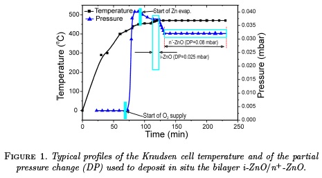
In a paper published previously by our group [21], a similar procedure was reported based on the reactive evaporation method to deposit in situ bilayers of i-ZnO/n-ZnO with opto-electric properties suitable for their use as optical windows in CuInS2 based solar cells. There the ZnO deposition process was controlled by an electronic system with facilities to perform sequential control of the Knudsen cell temperature and of the pressure change DP through PID algorithms. Taking into account that this system does not allow a precise control of DP, our group has developed an advanced control system that includes a combination of algorithms PID and PWM which achieved control of DP with high level of precision. The improvement of the DP control allowed depositing ZnO thin films with better opto-electrical properties and a greater reproducibility of thickness, transmittance and resistivity.
3. Results and Discussion
The opto-electrical properties of the ZnO films were optimized through a study on the influence of the main deposition parameters on both, the electric conductivity a and transmittance T. The best deposition conditions were obtained through a figure of merit FM that includes both the transmittance and resistivity, defined by the relation FM = -1/Ρ ln(T) [22]. The study revealed that the amount of Zn reaching the reactor (determined by the change of pressure DP), the O2-flow and the glow discharge current I affect both the transmittance and the resistivity of the ZnO films. Fig. 2 shows the influence of DP, I and O2-flow on Ρ, T and FM.
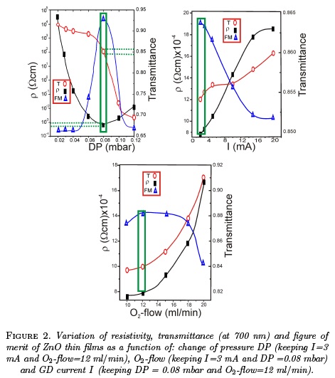
The transmittance measurements were carried out using a Varian-Cary 5000 spectrophotometer, the film thickness was determined using a Veeco Dektak 150 surface profiler. The electrical conductivity was measured using the four-probe method and the carrier concentration and Hall mobility were calculated from Hall voltage and electric conductivity measurements carried out using a procedure based on the Van Der Paw method and the ASTM F76 standard [23]. A magnetic field of 10 kG and the Keithley Hall effect equipment constituted by the commutation system 7001 and the Hall card 7065 were used to that effect. Based on the results presented in Fig. 2 we can highlight the following facts:
The three studied parameters affect both the transmittance and the resistivity of the ZnO films, being DP the parameter that most strongly affects these two properties. By properly selecting the values of DP, I and O2-flow and programming the deposition system following a routine of deposition as the one shown in Fig. 1, it is possible to grow in situ highly transparent i-ZnO and n+-ZnO films with resistivities less than 10-3 Ωcm for n+-ZnO films and greater than 104 Ωcm for i-ZnO films.
The increase in the GD current leads to an increase in the resistivity of the ZnO films, indicating that the increase of the ions energy caused by the increase of the GD voltage, that occurs when the current is increased, gives rise to an increase in the ratio of oxygen ions with respect to the zinc ion and therefore to a reduction of oxygen vacancies.
The increase in Zn (determined by the increase of DP) and/or decrease of oxygen in the plasma region, lead to a decrease of the resistivity, because in both cases there takes place an increase of the relation of zinc ions with respect to that of oxygen ions and, consequently, to an increase of the oxygen vacancies. The rapid decrease of resistivity observed when DP increases from 0.02 to 0.08 mbar, has been attributed to an increase of the density of free carriers associated to a decrease of oxygen vacancies, generated as a consequence of an increase of the Zn -ions to O2-ions ratio [21].
In samples prepared with excess Zn, the conductivity and the transmittance strongly decrease as the amount of Zn increases over values corresponding to DP=0.008 mbar. This behavior has been associated to generation of a high density of defects caused by the presence of Zn in interstitial positions [21]. These defects give rise to a band of active states within the gap which contribute to photon absorption in the entire spectral range studied. On the other hand, the decrease of conductivity observed when DP is greater than 0.08 mbar, has been attributed to a decrease of the mobility [21], apparently due to scattering of free carriers with defects generated by Zn in interstitial positions. Fig. 3 displays curves of spectral transmittance corresponding to typical thin films of i-ZnO, n+-ZnO, Zn-rich n+-ZnO and i-ZnO/ n+-ZnO bilayer that were deposited using a deposition profile as the one shown in Fig. 1. It is observed that the i-ZnO and n+-ZnO films present transmittances greater than 85 % at λ > 600 nm, whereas the transmittance of the ZnO/n+-ZnO bilayer exhibits a lower transmittance and shows maxima and minima of less amplitude than the layer of n+-ZnO, indicating that the interface of the bilayer induces a loss of coherence of the rays that are involved in the multiple internal reflections that give rise to constructive and destructive interference. The transmittance of the i-ZnO layer does not present interference maxima and minima because it is very thin (around 50 nm). Results of Fig. 3 also reveal that the slope and intensity of the transmittance curve of the Zn rich n+-ZnO film are significantly lower than that of the layers of i-ZnO and n+-ZnO. The strong decrease of transmittance could be attributed to an absorption band within the gap, generated by crystal imperfections associated with interstitial Zn positions and Frenkel defects. Zn in interstitial positions, additionally, produces mechanical deformation of the lattice, which leads to formation of states in tails of bands that extend into the gap, causing a decrease of the slope of the transmittance curves by increasing DP.

The absorption coefficient measured near the band edge (αE) has an exponential dependence on Urbach energy EU and hv, according the relation [24]:  where EU is related to the width of the band tail and E\ and a0 are constants; therefore, the Urbach energy can be obtained from the reciprocal slope of the linear part of the ln(αE) vs. hv plot. In Fig. 4 are displayed curves of ln(aE) vs. hv corresponding to ZnO films deposited varying DP, as well as the corresponding calculated values of EU. The absorption coefficient αE was calculated by a procedure based on the method of Swanepoel [25] and the experimental transmittance values shown in Fig. 3. Considering that the increase of Urbach energy is associated with an increase in the density of structural defects and that the Urbach energy of the ZnO films increases when the value of DP increases, we can conclude that, to deposit ZnO films with improved structural properties, it is convenient to use the lowest possible relationship of Zn ions with respect to the ion of O2, without affecting significantly the optimal values of transmittance and resistivity.

The ZnO films were also electrically characterized to identify the transport mechanisms that influence the electrical conductivity. The characterization was done through measurements of conductivity σ, Hall mobility µ and carrier concentration n in dependence of the temperature, in a range between 100 K and 600 K. Fig. 5 shows curves of σ as a function of temperature, carried out on typical n+-ZnO (103 Ω-1cm-:) and i-ZnO (10-2 Ω-1cm-:) samples. Curves of ln a vs. 1000/T are also plotted (see inset of Fig. 5).

It is noted that the conductivity of the i-ZnO film increases with increasing temperature, indicating a typical behavior of semiconductor materials, while the conductivity of the n+-ZnO film decreases (in most of the studied temperature range) with increasing temperature, which is a typical behavior of metals. The behavior of highly conductive n+-ZnO thin films can be explained considering that in highly conductive ZnO films the Fermi level is located within the conduction band since it is an n degenerate type semiconductor. The decrease in conductivity with temperature increase can be attributed to a decrease in mobility caused by interaction of free carriers with phonons. In degenerate semiconductors the reduction in mobility by increasing the temperature, predominates over the increase in conductivity by increasing the concentration of carriers with the temperature since most of the donor impurities are ionized at low temperatures.
The increase in the conductivity observed when the temperature increased from 400 K to 500 K (see inset in Fig. 5-b) can be explained by an increase in the density of free carriers, apparently induced by desorption of oxygen absorbed superficially. The results of Fig. 6 confirm this assertion. The activation energy ΔE = EC - EF, estimated from the slope of the curves of ln σ vs. 1000/T, is 0.05 eV, indicating that the energy of excitation for superficially absorbed oxygen is very small.

In high resistive i-ZnO samples, the curves of σ vs. T present two different slopes, indicating that the conductivity is affected by two different transport mechanisms, each one dominant in a different temperature range. On the other hand, the curve of ln σ vs. 1000/T can be expressed by the ratio σ = σ0 exp[-(EC - EF)/(kT)] which means that the conductivity is affected predominantly by carrier transport in extended states of the conduction band. At temperatures below 400 K, the increase of the conductivity is mainly caused by an increase in the density of free carriers coming from donor impurities (vacancies of oxygen), while at temperatures greater than 400 K, the increase of conductivity is caused by an increase in the density of free carriers, apparently induced by desorption of superficially chemisorbed oxygen. For i-ZnO films, activation energies of 0.04 eV and 0.45 eV in the ranges of low and high temperature were obtained respectively, indicating that in this type of samples the excitation energy for superficially absorbed oxygen is much greater than in n+-ZnO samples.
In Fig. 6 are plotted curves of Hall mobility and carrier concentration (determined from de relation σ = qnµ) as a function of the temperature; these results were obtained from measurements carried out to the n+-ZnO film whose curve of a vs T is showed in Fig. 5-b. The carrier concentration varies between 8 cm 3 and 12 x 1019 cm-3, being the increase very pronounced at temperatures higher than 400 K as a result of the desorption of superficial oxygen. The mobility generally decreases with increasing temperature as a result of the dispersion that free carriers undergo when interacting with phonons. However, when the temperature rises between 400 K and 500 K a strong decrease of the mobility is observed. This behavior could be associated to grain boundary effects induced by the trapping of carriers in grain boundaries states. This fact causes an increase of the potential barrier in grain boundaries, which gives rise to a strong decrease of mobility.
4. Conclusions
A novel procedure based on the reactive evaporation method was developed to deposit highly transparent thin films of i-ZnO and n+-ZnO. Through an optimized reactor design and an exhaustive study of preparation parameters, conditions were found to deposit in-situ the bilayer i-ZnO/n+-ZnO with thicknesses and opto-electric properties suitable for their use as optical solar cell windows. Resistivities of 6x 10⁻⁴ Ωcm and 104 Ωcm were obtained for n+-ZnO and i-ZnO respectively without using extrinsic doping. The high conductivity of n+-ZnO films is mainly caused by a high density of free carriers (∼ 8 x 1019 cm-3) generated by oxygen vacancies.
Very good reproducibility of the thickness and opto-electrical properties of the layers constituting the i-ZnO/n+-ZnO bilayer was achieved through a novel electronic control which includes a PID algorithm to control the temperature of the Knudsen cell in a temperature range between 20 °C and 400 °C, followed by a PWM algorithm to control the rate of evaporation of Zn at temperatures greater than 400 °C.
We found that n+-ZnO thin films deposited under excess Zn (DP> 0,8) have poor transmittance and conductivity, apparently caused by a high density of defects associated to precipitation of Zn in interstitial positions. From Urbach energy measures was additionally found that ZnO films deposited using DP values lower or equal to 0.08 have a low density of structural defects.
The reactive evaporation system used in this work has some advantages compared to the rf sputtering method generally used to grow ZnO films used as solar cell optical windows. Among others, it is worth mentioning the following: allows to grow n+-ZnO films without incorporating doping impurities, which has advantages in an industrial production process; allows depositing ZnO films with opto-electrical properties similar to those obtained by rf-sputtering but at a lower cost, especially for large areas, due to the high cost of the ceramic targets used in rf sputtering.
Acknowledgments
This work was supported by Colciencias (Contract #038/2013) and Universidad Nacional de Colombia, Bogotá, DIB (Proy. 20287).
References
[1] M. Islam, S. Ishizuka, A. Yamada, K. Matsubara, S. Niki, T. Sakurai, and K. Akimoto, Appl. Surf. Sci. 257, 4026 (2011).
[2] J. A. Shama, S. Johnston, T. Moriarty, G. Teeter, K. Ramanathan, and R. Nuofi, Prog. Photovolt: Res. Appl. 12, 39 (2004).
[3] D. Aaron, R. Barkhouse, O. Gunawan, T. Gokmen, T. K. Todorov, and D. B. Mitzi, Prog. Photovolt: Res. Appl. 20, 6 (2012).
[4] N. Yong-Jin, N. Seok-In, and K. Seok-Soon, Sol. Energy Mater. Sol. Cells 117, 139 (2013).
[5] W. Jen-Chun, W. Wei-Tse, T. Meng-Yen, L. Ming-Kun, H. Sheng-Fu, P. Tsong-Pyng, K. Chi-Chung, Y. Chih-Chieh, and M. Hsin-Fei, J. Mater. Chem. 20, 862 (2010).
[6] P. P. Boix, K. Nonomura, N. Mathews, and S. Mhaisalkar, Materials Today 17, 16 (2014).
[7] D. Liu and T. Kelly, Nat. Photon. 8, 133 (2014).
[8] C. H. Chen, Y. C. Chen, S. F. Hong, C. L. Wang, W. C. Shih, C. P. Tsai, Y. C. Wu, C. H. Lai, C. N. Wei, and H. Y. Bor, Proc. 35th IEEE photovoltaic Specialist Conf. , 2413 (2010).
[9] R. Menner, D. Hariskos, V. Linss, and M. Powalla, Thin Solid Films 519, 7541 (2011).
[10] T. M. Barnes, J. Leaf, C. Fry, and C. A. Wolden, J. Cryst. Growth 274, 412 (2005).
[11] M. Kauk, K. Muska, M. Altosaar, M. Danilson, K. Ounpuu, T. Varema, and O. Volobujeva, Proc. 35th IEEE photovoltaic Specialist Conf. , 2452 (2010).
[12] M. Caglar, S. Ilican, Y. Caglar, and F. Yakuphanoglu, J. Mater Sci - Mater Electron 19, 704 (2008).
[13] M. Ristic, S. Music, M. Ivanda, and S. Popovic, J. Alloys Compd. 397, L1 (2005).
[14] pvtech, "http://www.pvtech.org/news/hanergysjsolibroJias_20.5_cigs_solar_celLverified_by_nrel," (2014).
[15] D. Yuvaraj and K. Narasimha, Vacuum 82, 1274 (2008).
[16] D. Yuvaraj, M. Sathyanarayanan, and K. N. Rao, Applied Nanoscience 4, 801 (2014).
[17] R. Bishop, Learning with LabVIEW 8 (Pearson Prentice Hall, 2007).
[18] A. Fridman, Plasma Chemistry (Cambridge University Press, 2008).
[19] A. von Engel, Electric plasmas: their nature and uses (Taylor and Francis Ltda, 1983).
[20] G. Gordillo, A. A. R. Botero, and E. A. Ramirez, J. Mater. Res. Technol., Accepted for publication, in press https://doi.org/10.1016/j.jmrt.2015.11.004 (2015).
[21] J. Oyola, J. Castro, and G. Gordillo, Sol. Energy Mater. Sol. Cells 102, 137 (2012).
[22] V. K. Jain and A. P. Kulshreshtha, Solar Energy Materials 4, 151 (1981).
[23] S. P. et al., Annual Book of ASTM Standards, Vol. 10.05 (American Society for Testing and Materials, 1991).
[24] S. Ilican, Y. Caglar, M. Caglar, and B. Demirci, J. Optoelectron. Adv. Mater. 10, 2578 (2008).
[25] R. Swanepoel, J. Phys. E: Sci. Instrum. 16 (1983).
How to Cite
APA
ACM
ACS
ABNT
Chicago
Harvard
IEEE
MLA
Turabian
Vancouver
Download Citation
License
Those authors who have publications with this journal, accept the following terms:
a. The authors will retain their copyright and will guarantee the publication of the first publication of their work, which will be subject to the Attribution-SinDerivar 4.0 International Creative Commons Attribution License that permits redistribution, commercial or non-commercial, As long as the Work circulates intact and unchanged, where it indicates its author and its first publication in this magazine.
b. Authors are encouraged to disseminate their work through the Internet (eg in institutional telematic files or on their website) before and during the sending process, which can produce interesting exchanges and increase appointments of the published work.