Published
DEPENDENCE OF PHOTONIC BAND GAP ON THE RADIUS OF TRACES IN TiO2 NANOSTRUCTURES
DEPENDENCIA DEL GAP FOTÓNICO CON EL RADIO DE LAS HUELLAS EN NANOESTRUCTURAS DE TiO2
DOI:
https://doi.org/10.15446/mo.n55.66141Keywords:
Photonic crystals, Titania, TiO2 traces (en)Cristal fotónico, Dióxido de titanio, Huellas de TiO2 (es)
We study the evolution of the photonic gap present in TiO2 traces, these structures appear in the Ti-TiO2 interface during titania nanotubes formation. Traces can be modeled like photonic crystal because the dielectric function varies periodically in a bi-dimensional space. We conducted a theoretical study based on experimental measurements in traces of TiO2. The study was developed using a plane wave expansion method. This work is a first attempt to introduce photonic gap engineering, which could have technological interests.
Recibido: de noviembre de 2016; Aceptado: de marzo de 2017
Abstract
We study the evolution of the photonic gap present in TiO2 traces, these structures appear in the Ti-TiO2 interface during titania nanotubes formation. Traces can be modeled like photonic crystal because the dielectric function varies periodically in a bi-dimensional space. We conducted a theoretical study based on experimental measurements in traces of TiO2. The study was developed using a plane wave expansion method. This work is a first attempt to introduce photonic gap engineering, which could have technological interests.
Keywords:
Photonic crystals, Titania, TiO2 traces.Resumen
Se estudió la evolución de la brecha de frecuencias fotónicas presente en las huellas de TiO2, estas estructuras aparecen en la interfaz Ti-TiO2 durante la formación de nanotubos de óxido de titanio. Las huellas se pueden modelar como un cristal fotónico debido a que la función dielectrica varía periodicamente en un espacio bi-dimensional. Hemos llevado a cabo un estudio teórico sobre la base de mediciones experimentales en las huellas de TiO2. El estudio se desarrolló mediante el uso del método de expansión en ondas planas. Este trabajo es un primer intento para introducir una ingeniería de brecha fotónica, lo cual puede tener interés tecnológico.
Palabras clave:
Cristal fotónico, Dióxido de titanio, Huellas de TiO2.Introduction
In the last decades, new materials with large possibilities of technological applications have appeared as a direct consequence of developments in nanoscience. These materials exhibit novel optic, electronic or magnetic properties among others. Among these systems, the photonic materials can manipulate and control the transport of light. In fact, photonic crystals are considered equivalent to semiconductors for the light.[1] The term photonic crystals was introduced in 1987 by Yablonovitch and John. [2,3] In the last years, there are many expectations on photonic crystals regarding their uses and applications in different fields of knowledge and technology, like medicine, optics, optoelectronics, and telecommunications. An important characteristic of photonic systems is the versatility to be grown in one, two or three dimensions that should permit its integration in optoelectronic devices.
Photonic crystals use the periodic variation of the dielectric function to control the light in a similar way that in crystals happen with the electrons. Generally, photonic crystals are a material or matrix with dielectric constant Є1, where there are immersed an array of forms made of a second material with dielectric constant Є2. This picture resembles the atomic organization of a crystal where the space is the first material and the atoms correspond to the second material. So, traditional concepts from electronic band theory are useful in this subject. However, light does not obey the Fermi-Dirac statistics and the second material, "the atoms" can have different shapes: circular, square and triangular, to mention a few examples. Another difference is that there are two different components in the dispersion relation: Transverse Electric and Transverse Magnetic modes. For this reason it is possible to have photonic band gap (PBG) for either both modes or one of them. The PBG is a function of the geometric properties of the photonic crystal and the difference between the dielectric constants. These characteristics are a powerful tool to develop photonic devices for possible technological applications.
In a recent paper was reported the formation of TiO2 nanostructures as a secondary effect during the grow of TiO2 nanotubes[4] for the anodization method. [5] These nanostructures that we will call as traces appeared on the Ti surface and can be visible after remove the nanotubes by mechanical stress. The traces resemble an egg box and present photonic properties. TiO2 Anatase and Rutile phases were identified in the traces. This work sought to bring a connection between the relevant parameters of the PGB with the radii of the circular forms of traces.
We used a representation of the traces as a photonic system where long cylindrical rods of air were immersed in a TiO2 matrix. In the xy plane the rods were distributed in a hexagonal array such that a 2D system was formed. The dielectric function remained constant in the z direction. This picture was inspired by SEM micrographs from traces, as we can see in Fig 1(a). Numerical experiments were developed in order to explore the effect produced on PBG when radius of traces changed.

FIGURE 1:
(a) SEM micrograph of TiO2 traces and the nanotuhes. In i, ii and iii panels the traces can he better observed. (b) Reconstruction of traces from SEM images.
In particular, we studied the evolution of the position and the width of the first partial gap as a function the radii of traces considering both Anatase and Rutile phases for the M and K symmetry points. The traces packing factor dependence with the radii of TiO2 traces was determinate. These calculations would enable the acquisition of information to prepare materials with specific characteristics, suitable for practical applications.
Experimental Details
The traces were obtained during TiO2 nanotube fabrication via mechanical stress of titanium foils [6]. The nanotubes were obtained by electrochemical anodization of titanium foils of 2 x 4 cm, 50 m thickness and 99.96% pure used as anode and cathode in a solution of ethylenglicol, distilled water, and ammonium fluoride (NH4F). The applied voltage was alternated between 80 and 20 V for 2 h. [6]
Figure 1 shows the SEM micrograph of the traces and their reconstruction. Figure 1b) is the reconstruction of the traces' topography from SEM micrographs, evidencing the honeycomb formation: one trace accompanied for 6 neighboring. This is associated to the self-organization of the nanotubes by anodized process. [6] The reconstruction was realized through to the transform the 2D image uses pixel width, height, and voxel depth as scaling factors to convert voxel coordinates, in this case the scale for the voxel is nm. Height and volume of the image are created by using the alpha value in the Transfer Function that indicates the transparency of every pixel, depending on its intensity. Pixels with low intensity values are usually more transparent (low alpha), while pixels with high intensity values are more opaque (high alpha). [7]
Figure 1a) shows the topography of traces in different regions: regions i and ii evidence deformations in the traces associated to the imperfections in the titanium foils, replicated during the formation of the nanotubes after anodizing; while region iii shows the self-ordered traces reconstructed in Figure 1b), evidencing that the traces have a honeycomb formation.
0.1. Theoretical Model
From Maxwell equations and considering the absence of external currents and sources, it is possible to find a master equation that governs the study of photonic crystals [8-12] given for Eq. (1):

This equation represents a linear Hermitian eigenvalue problem, where the term inside of parenthesis is the Hermitian differential operatorΘ. Its solution implies a variational approach, where each eigenvalue is computed separately by minimizing the functional 〈Hn|Θ|Hn〉.[3] In this method, the electric and magnetic fields are expanding into a set of harmonic modes. The solutions of Eq. (1) depend of the dielectric function Є(r) properties than in the present model varies in two dimensions forming a 2D photonic crystal where the air cylindrical rods form a hexagonal pattern. In 2D photonic lattices appear two principal non degenerated components of the electromagnetic field: transverse magnetic (TM), and transverse electric (TE) modes. [13,14]
Traces are modeled as a bi-dimensional system forms by a TiO2 matrix, in the Anatase ( Є = 5.62 [13,14]) and Rutile ( Є = 6.33 [13,14]) phases and air cylinders inside them. The parameters used for the simulation using the MIT Photonic-Bands (MPB) [15,16] code are: lattice parameter a=100nm, radii of traces varying between 12 nm and 42nm, and for numerical optimization a grid size of 100 x 100 points, 12 bands and 900 points in the reciprocal space for the dispersion relation were used. Γ= (0, 0,0), M= ( ) and K= (
 ) were the respective high symmetry points used. To conduct the study, we began from the experimental measurement of the traces (83.53 ± 1.93 nm), establishing the radii of 42nm as reference to perform the simulations.
Results and Discussion
This theoretical study sought to identify the evolution of partial gaps of the TE and TM modes as a function of the size of the radius of TiO2 traces. This artificial material exhibits a photonic behavior and presents a hexagonal array, which has the matrix of Anatase and Rutile phases (black) with air cylinders in the representation of TiO2 traces (white) Fig. 2(a-d), with radii of cylinders varying from 12 nm to 42 nm. When the radius of traces increases, the packing factor
PF
, the relation between the occupied area of air cylinders and TiO2 matrix increases with a quadratic behavior, following the equation P
F
=
2Πr2
/( ), r ≤ 2a , which is for 2D hexagonal lattices. The packing factor is shown in Fig. 2(e). The photonic band structures obtained for Anatase and Rutile phases are shown in Figs. 4 to 7 for radii of 12 nm, 22 nm, 32 nm, and 42 nm, respectively.

Figure 2:
Schematic representation of the traces for different radii: (a) r = 12 nm, (b) r = 22 nm, (c) r = 32 nm, (d) r = 42 nm, (e) Variation of the packing factor with the radius of traces.
The increase of the partial gap of TE mode (TE) is shown for both phases of TIO2. This region defines the frequencies in which the light cannot propagate in the periodical photonic crystal of TiO2-air implemented in this study. When the radii of traces are small (r = 12nm. Fig. 2(a)), in comparison to reference radius of 42nm (Fig. 2 (d)), the gap region is not open; the dielectric and air band has a very close frequency value, which inhibits the appearance of gaps (Fig. 3).

Figure 3:
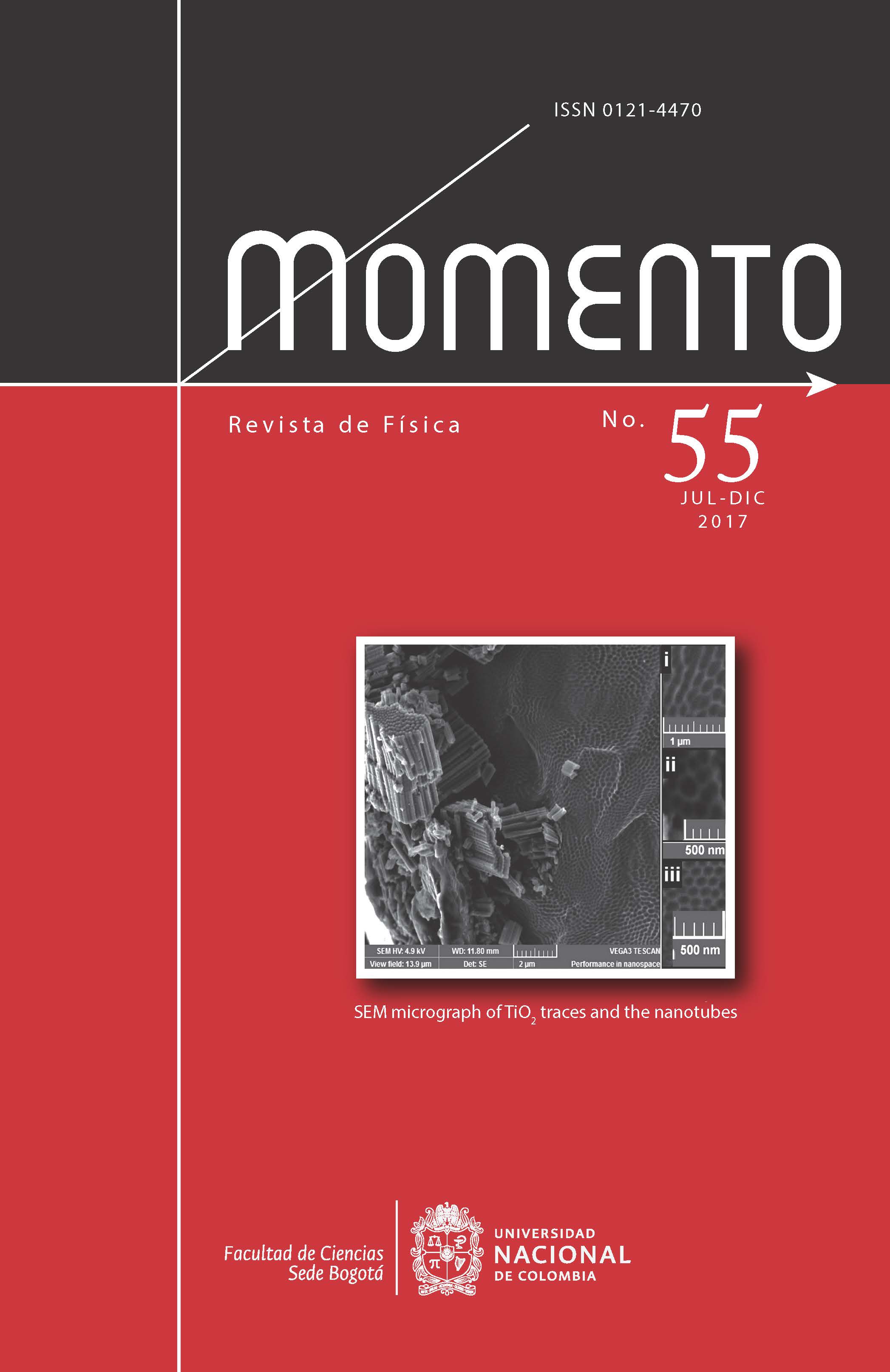
Photonic hand structure, TE modes (red) and TM modes (violet), for a honeycomh lattice model with a matrix of Anatase (a) and Rutile (b) phases of TiO2 and traces with radii r = 12nm.
Figure 6 shows the maximum value of the photonic band gap region, corresponding to the radius taken as reference. This value is obtained from SEM micrographs of TiO2 nanotubes. [6] For this case, the first band gap for TE modes has an interesting property: the lowest state of second band occurs at M point while the highest state of first band is at K point. This behavior is similar as the indirect electronic gap in semiconductors. For this reason, the effectively gap for light transportation must take in account this characteristic. However, photons obey Bose-Einstein statistics and direct-like transitions can happen. This effective gap disappears for radius lower than 22 nm even that at K or M point is possible to observe a local gap, see Figs. 3 to 6.
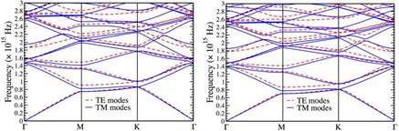
Figure 4:
Photonic hand structure, TE modes (red) and TM modes (violet), for a honeycomh lattice model with a matrix of Anatase (a) and Rutile (b) phases of TiO2 and traces with radii r = 22nm.
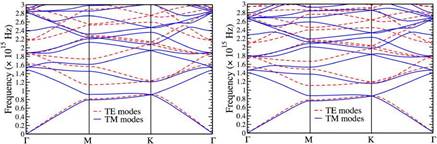
Figure 5:
Photonic hand structure, TE modes (red) and TM modes (violet), for a honeycomh lattice model with a matrix of Anatase (a) and Rutile (b) phases of TiO2 and traces with radii r = 32nm.
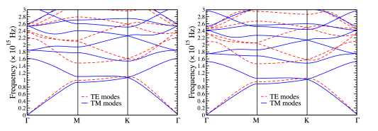
Figure 6:
Photonic hand structure, TE modes (red) and TM modes (violet), for a honeycomb lattice model with a matrix of Anatase (a) and Rutile (b) phases of TiO2 and traces with radii r = 42nm.
The evolution of the central frequency of the local gap, for M and K point, as function of radius in Anatase and Rutile phases are shown in Figs. 7. Local gap at K point is higher than local gap at M point for both modes and phases.

Figure 7: Dependence of central frequency value on the radii of traces in the first partial gap of TE (Left panel) and TM (Right panel) modes for Anatase and Rutile phases in M and K high symmetry points.
Conclusions
A study of the effect of the change in the radii of TiO2 traces on the properties of gaps for a 2D photonic material compose of Titania (Anatase and Rutile phases) - air hole was conducted. From them, it is possible to determine that the value of the photonic gap increases, according to the radii increase. This behavior is observed both K and M high symmetry points. In the same form, the photonic gap could be tuned with the packing factor which can be considered a new tool more useful in technology applications. Our results predict a threshold of 150 Thz for the maximum value of the central frequency of the first photonic gap when the packing factor reaches the maximum value of 0.906 for a 2D hexagonal lattice.
Acknowledgements
This work was partially supported by the Universidad Nacional de Colombia - DIB projects Quipú codes 201010020493, 201010021532 and 201010026656. Also, it was partially financed by Colciencias, project code Quipú No. 201010019609.
References
References
E. Yablonovitch, Phys. Rev. Lett. 58, 2059 (1987).
S. John, Phys. Rev. Lett. 58, 2486 (1987).
A. Tan, B. Pingguan-Murphy, R. Ahmad, and S. Akbar,
Ceram. Int. 38, 4421 (2012).
J. Joannopoulos, S. Johnson, J. Winn, and R. Meade,
Photonic Crystals: Molding the Flow of Light (Princeton
University Press, 2011).
H. P. Quiroz and A. Dussan, in Key Engineering Materials V ,
Dependence of photonic band gap on the radius of traces in TiO2 nanostructures 35 Adv. Mater. Res., Vol. 1119 (Trans Tech Publications, 2015) pp. 121{125.
H. P. Quiroz and A. Dussan, J. Appl. Phys. 120, 051703
(2016).
K. Inoue and K. Ohtaka, Photonic Crystals: Physics,
Fabrication and Applications, Springer Series in Optical
Sciences (Springer Berlin Heidelberg, 2004).
C. Soukoulis, Photonic Band Gap Materials, Nato Science
Series E: (Springer Netherlands, 2012).
J. Joannopoulos, S. Johnson, J. Winn, and R. Meade,
Photonic Crystals: Molding the Flow of Light (Princeton
University Press, 2011).
D. Pagnoux, J. Lourtioz, P. de Fornel, H. Benisty, V. Berger,
J. Gerard, D. Maystre, and A. Tchelnokov, Photonic
Crystals: Towards Nanoscale Photonic Devices (Springer
Berlin Heidelberg, 2008).
P. Hohenberg and W. Kohn, Phys. Rev. 136, B864 (1964).
K. M. Ho, C. T. Chan, and C. M. Soukoulis, Phys. Rev. Lett.
, 3152 (1990).
S.-D. Mo and W. Y. Ching, Phys. Rev. B 51, 13023 (1995).
C. P. Barrera-Pati~no, H. P. Quiroz, R. R. Rey-González, and A. Dussan, Adv. Mater. Lett. 7, 802 (2016).
MIT Photonic Bands - AbInitio," (2017), http://ab-initio.
mit.edu/wiki/index.php/MIT Photonic Bands.
S. G. Johnson and J. D. Joannopoulos, Opt. Express 8, 173
(2001).
How to Cite
APA
ACM
ACS
ABNT
Chicago
Harvard
IEEE
MLA
Turabian
Vancouver
Download Citation
CrossRef Cited-by
1. C. P. Barrera-Patiño, J. D. Vollet-Filho, R. G. Teixeira-Rosa, H. P. Quiroz, A. Dussan, N. M. Inada, V. S. Bagnato, R. R. Rey-González. (2020). Photonic effects in natural nanostructures on Morpho cypris and Greta oto butterfly wings. Scientific Reports, 10(1) https://doi.org/10.1038/s41598-020-62770-w.
Dimensions
PlumX
Article abstract page views
Downloads
License
Copyright (c) 2017 MOMENTO

This work is licensed under a Creative Commons Attribution-NoDerivatives 4.0 International License.
Those authors who have publications with this journal, accept the following terms:
a. The authors will retain their copyright and will guarantee the publication of the first publication of their work, which will be subject to the Attribution-SinDerivar 4.0 International Creative Commons Attribution License that permits redistribution, commercial or non-commercial, As long as the Work circulates intact and unchanged, where it indicates its author and its first publication in this magazine.
b. Authors are encouraged to disseminate their work through the Internet (eg in institutional telematic files or on their website) before and during the sending process, which can produce interesting exchanges and increase appointments of the published work.