AlN film deposition as a semiconductor device
Deposición de películas de AlN como dispositivos semiconductores
DOI:
https://doi.org/10.15446/ing.investig.v33n2.39505Keywords:
Pulsed laser deposition, aluminium nitride, acoustic wave speed (en)nitruro de aluminio, deposición de láser pulsado, reflectancia óptica, pureza del color, respuesta de frecuencia, velocidad de la onda acústica (es)
AlN films were deposited by pulsed laser deposition (PLD) using an Nd: YAG laser (λ = 1064 nm). The films were deposited in a nitrogen atmosphere as working gas; the cathode was an aluminium high purity (99.99%) target. The films were deposited using 7 J/cm2 laser fluence for 10 minutes on silicon (100) substrates. The working pressure was 9x10⁻³ mbar and the substrate temperature was varied from 200°C to 630°C. The thickness measured by profilometer was 150 nm for all films. Moreover, surface acoustic wave (SAW) devices with a Mo/AlN/Si configuration have been fabricated using AlN-buffer and Mo Channel. The films’ morphology and composition were studied using scanning electron microscopy (SEM) and energy dispersive X-ray analysis (EDX), respectively. The films’ optical reflectance spectra and colour coordinates were obtained by optical spectral reflectometry in the 400-900 cm-1 range using an Ocean Optics 2000 spectrophotometer. The present work found clear dependence on morphological properties, reflectance, dominant wavelength colour purity, frequency response and acoustic wave speed in terms of the temperature applied to the substrate. About 30% reduction in reflectance was observed and increased acoustic wave speed of about 1.3 % when the temperature was increased from 200°C to 630°C.
Películas de AlN fueron depositados por la técnica de deposición por láser pulsado (PLD), utilizando un láser Nd: YAG con una longitud de onda de 1064 nm. Las películas fueron depositadas en una atmósfera de nitrógeno como gas de trabajo; como cátodo se usó aluminio de alta pureza (99,99%). Las películas fueron depositadas con una fluencia del láser de 2,28 J/cm2 durante 10 minutos sobre sustratos de silicio (100). La presión de trabajo fue de 9 x 10⁻³ mbar y la temperatura del sustrato se varió desde 200 °C a 630 °C. El espesor medido por perfilometría fue de 150 nm para todas las películas. Además se fabricaron los dispositivos de ondas acústicas de superficie (SAW) con una configuración Mo/AlN/Si, empleando AlN-bufer y un canal de Mo. La morfología y la composición de las películas se estudiaron mediante microscopía electrónica de barrido (MEB) y energía dispersiva de rayos X de análisis (EDX), respectivamente. Los espectros de reflectancia óptica y color de coordenadas de las películas se obtuvieron por la técnica óptica reflectometría espectral en el rango de 400-900 cm-1 por medio de un espectrofotómetro Ocean Optics 2000. En este trabajo se encontró una clara dependencia de las propiedades morfológicas, reflectancia, pureza dominante, longitud de onda del color, la respuesta de frecuencia y velocidad de la onda acústica en términos de la temperatura aplicada al sustrato. Se observó una reducción en la reflectancia de aproximadamente 30% y aumento de velocidad de la onda acústica de aproximadamente 1,3% cuando la temperatura se incrementó desde 200 °C a 630 °C.
J. C. Caicedo1, J. A. Pérez2 and W. Aperador3
1 Julio Cesar Caicedo. Ingeniero de Materiales and Doctor en Ingeniería, Universidad del Valle, Colombia. Affiliation: Universidad del Valle, Colombia.
E-mail: jcaicedoangulo1@gmail.com
2 Jaime Andrés Pérez Taborda. Ingeniería Física, Universidad Tecnológica De Pereira, Colombia. Máster oficial radiación de sincrotrón y aceleradores de partículas, Universidad Autónoma de Barcelona, España. Affiliation: Universidad Tecnológica de Pereira, Colombia. E-mail: j.a.perez@gmail.co
3 Willian Aperador Chaparro. Físico and Magister en Metalurgia y Ciencia de los Materiales, Universidad Pedagógica y Tecnológica de Colombia, Colombia. Doctor en Ingeniería, Universidad del Valle, Colombia. Affiliation: Universidad Militar Nueva Granada, Colombia. E-mail: g.ing.materiales@gmail.co
How to cite: Caicedo, J. C., Pérez, J. A., Aperador, W., AlN film deposition as a semiconductor device., Ingeniería e Investigación. Vol. 33, No. 2. August 2013, pp. 16 – 23.
ABSTRACT
AlN films were deposited by pulsed laser deposition (PLD) using an Nd: YAG laser (λ = 1064 nm). The films were deposited in a nitrogen atmosphere as working gas; the cathode was an aluminium high purity (99.99%) target. The films were deposited using 7 J/cm2 laser fluence for 10 minutes on silicon (100) substrates. The working pressure was 9x10⁻³ mbar and the substrate temperature was varied from 200°C to 630°C. The thickness measured by profilometer was 150 nm for all films. Moreover, surface acoustic wave (SAW) devices with a Mo/AlN/Si configuration have been fabricated using AlN-buffer and Mo Channel. The films’ morphology and composition were studied using scanning electron microscopy (SEM) and energy dispersive X-ray analysis (EDX), respectively. The films’ optical reflectance spectra and colour coordinates were obtained by optical spectral reflectometry in the 400-900 cm-1 range using an Ocean Optics 2000 spectrophotometer. The present work found clear dependence on morphological properties, reflectance, dominant wavelength colour purity, frequency response and acoustic wave speed in terms of the temperature applied to the substrate. About 30% reduction in reflectance was observed and increased acoustic wave speed of about 1.3 % when the temperature was increased from 200°C to 630°C.
Keywords: Pulsed laser deposition, aluminium nitride, acoustic wave speed.
RESUMEN
Películas de AlN fueron depositados por la técnica de deposición por láser pulsado (PLD), utilizando un láser Nd: YAG con una longitud de onda de 1064 nm. Las películas fueron depositadas en una atmósfera de nitrógeno como gas de trabajo; como cátodo se usó aluminio de alta pureza (99,99%). Las películas fueron depositadas con una fluencia del láser de 2,28 J/cm2 durante 10 minutos sobre sustratos de silicio (100). La presión de trabajo fue de 9 x 10⁻³ mbar y la temperatura del sustrato se varió desde 200 °C a 630 °C. El espesor medido por perfilometría fue de 150 nm para todas las películas. Además se fabricaron los dispositivos de ondas acústicas de superficie (SAW) con una configuración Mo/AlN/Si, empleando AlN-bufer y un canal de Mo. La morfología y la composición de las películas se estudiaron mediante microscopía electrónica de barrido (MEB) y energía dispersiva de rayos X de análisis (EDX), respectivamente. Los espectros de reflectancia óptica y color de coordenadas de las películas se obtuvieron por la técnica óptica reflectometría espectral en el rango de 400-900 cm-1 por medio de un espectrofotómetro Ocean Optics 2000. En este trabajo se encontró una clara dependencia de las propiedades morfológicas, reflectancia, pureza dominante, longitud de onda del color, la respuesta de frecuencia y velocidad de la onda acústica en términos de la temperatura aplicada al sustrato. Se observó una reducción en la reflectancia de aproximadamente 30% y aumento de velocidad de la onda acústica de aproximadamente 1,3% cuando la temperatura se incrementó desde 200 °C a 630 °C.
Palabras clave: nitruro de aluminio, deposición de láser pulsado, reflectancia óptica, pureza del color, respuesta de frecuencia, velocidad de la onda acústica.
Received: Augus 12th 2012 Accepted: June 18th 2013
Introduction
Metal nitrides based on aluminum nitride (AlN) are of great interest because of their electrical, optical and acoustical properties (Men and Lin., 2006; Ristoscu et al., 2005). Their hardness and thermal coefficients of expansion are comparable to those of silicon (Si). AlN is used for acoustic wave devices on Si, optical coatings for spacecraft components, heat-sinks in electronic packaging applications, as well as electroluminescent devices in the wavelength range from 215 nm to the blue end of the optical spectrum (Ristoscu et al., 2005). Some optical properties near AlN’s fundamental band gap have been reported by Yamashita et al. since 1979 (Yamashita et al., 1979); several theoretical studies have been well documented (Christensen and Gorczyca, 1994; Hughes et al., 1997); however, reliable experimental data (Ristoscu et al., 2005) has been reported very recently because both sample quality and the spectroscopic techniques have only been substantially improved during recent years. Precise knowledge of the optical constants is particularly important in view of the use of AlN-based thin films in optical filters and light-emitting laser diodes since they also have temperature dependence (Jiang et al., 2003). Pulsed laser deposition (PLD) has been largely applied to processing thin films and other structures. PLD’s highly non-equilibrium nature is attractive for synthesising stoichiometric thin films of various metal nitrides, carbon nitrides, oxides and oxi-nitrides from the corresponding bulk targets. PLD appears to be a suitable method for transferring stoichiometrically complex monolayer structures from AlN ceramic structures to substrates. Many infra-red (IR) measurements presented in the literature were thus used to estimate AlN stoichiometric film quality. The IR spectra provided important information about the composition, homogeneity, crystallinity and residual stresses present in the films. Moreover, ellipsometric and reflectance measurements have been used for determining the refractive index in many AlN compounds, since ellipsometry and reflectance are sensitive and non-destructive techniques used for studying surface and thin film optical properties and microstructures (Ristoscu et al., 2005). Single-chip front-end RF modules incorporating surface acoustic wave (SAW) filters are a matter for intense research. At present, these modules are fabricated by bonding single crystal piezoelectric SAW devices onto integrated circuits. Thin polycrystalline aluminium nitride (AlN) films are promising materials for integrating SAW devices onto Si substrates due to their good piezoelectric properties and the possibility of deposition at low temperatures compatible with manufacturing Si integrated circuits. AlN thin films of sufficient quality for SAW applications can be obtained by the PLD technique (Clement et al., 2004). This work was thus aimed at studying the effect of deposition temperature on chemical, morphological optical properties, frequency response, and acoustic wave speed of binary AlN films deposited by PLD on Si (100) for use in optical and electronic applications. Fresh results regarding depositing AlN films from Al targets with nitrogen as working gas and their characterisation by X-ray photoelectron spectroscopy (XPS) are reported, along with reflectance investigation and scanning electron microscopy (SEM) results.
Experimental
PLD configuration consisted of a laser system, a multi-port stainless steel vacuum chamber equipped with a gas inlet, a rotating target and a heated substrate holder. A Nd:YAG laser was used providing the 1064 nm wavelength pulses, with 9 ns pulse duration and 10 Hz repetition rate . The laser beam was focused on the target with an f = 23 cm glass lens at 45° angle regarding normal. The target rotated at 2.2 rpm to avoid fast drilling. The distance between the target and substrate was 6.5 cm. Before deposition, the vacuum chamber was evacuated down to 1•10-5 mbar by using a turbo-molecular pump backed with a rotary pump. The films were deposited in a nitrogen atmosphere as working gas, using an aluminium target (99.99%) as metal source. Films were deposited with 7 J/cm2 laser fluence for 10 minutes on silicon substrates (100). The working pressure was 9•10-3 mbar and substrate temperature varied from 200°C to 630° C. The thickness of the films measured with a profilometer was 150 nm for all films; deposition time was 10 min for all films. An exhaustive XPS study was carried out for AlN films. XPS was used on AlN samples to determine their chemical composition and aluminium and nitrogen atom bonding using ESCA-PHI 5500 monochromatic Al Kα radiation and 0.1 eV passing energy. This technique’s surface sensitivity was so high that any contamination could produce deviation from the real chemical composition; the XPS analysis was therefore performed in ultra-high vacuum conditions with a sputter cleaning source to remove any undesired contaminants. The surface properties (grain size and roughness) were determined via atomic force microscopy (AFM-Asylum Research MFP-3D). The samples’ optical reflectance spectra and colour coordinates were obtained by spectral reflectometry in the 400–900 cm-1 range by means of an Ocean Optics 2000 spectrophotometer. The coated samples received white light from a halogen lamp illuminator through a bundle of six optical fibres; the light reflected on the samples was collected by a single optical fibre and analysed in the spectrophotometer. The fibre was fixed to the sample surface in a perpendicular direction. An aluminium mirror film freshly deposited by rapid thermal evaporation in high vacuum was used as the reference sample; experimental spectra were normalised to 100% reference sample reflectance. AlN surface film morphology and micro-device structure (SAW) was analysed by scanning electron microscopy (SEM) (Leika 360, Cambridge Instruments). SAW devices having different deposition temperatures, such as Mo/AlN/Si, were fabricated to estimate the effect of AlN buffer layers on their frequency response characteristics. Inter-digitated transducer (IDT) electrodes (Mo, 400 nm) having 80 finger pairs and 1 mm line width were designed by using a widely-used impulse response model and formed by using a lift-off method. Frequency response was measured by a network analyzer (HP 8720C), in terms of AlN film deposition conditions. Insertion loss at center frequency was monitored from the frequency responses and correlated with AlN film deposition temperature and surface roughness. SAW propagation was studied by analysing scattering parameters on Mo/AlN/Si transmission configurations.
Results and discussion
XPS analysis
Figure 1 shows XPS survey spectrum for AlN thin film grown at 300ºC. Peaks at 534.4 eV, 397.3 eV, 124.4 eV and 73.9 eV corresponded to O1s, N1s, Al2s, and Al2p binding energy, respectively. Calculating peak areas from deconvoluted spectra (Figure 2) without O1s contribution gives an atomic ratio of Al:N = 0.392:0.588, this being similar to Al0.40N0.60 stoichiometry (Rosenberger et al., 2008).

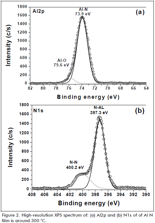
Core electron spectra carry information regarding Al–N film chemical composition and bonding characters. The integral of N1s, A2s, and Al2p spectra corrected by relevant sensitive factors can evaluate Al and N element concentrations in Al–N films. The corresponding deconvoluted peak integral can also be used for estimating bond content, described by the following formula (Zhuang et al., 2009):

where S was the sensitivity factor, A the integral of deconvoluted peaks and C atomic content. The numerator was the sum of the integral of one sort of bond; the denominator was the sum of the integral of all types of bonds decomposed from the whole peak for N1s, A2s, and Al2p in the sample. The atomic concentrations of Al, N and O elements from XPS analysis of the coating deposited at 300 °C are listed in Table 1. The O concentration was less than 3% for all Al-N films obtained (Wang et al., 2007).

Surface analysis of AlN films via AFM
Figure 3a-c shows a 5µm× 5µm image for AlN films deposited at differing deposition temperatures. The general trend in the AlN films with decreasing temperature revealed a decrease in grain size and roughness. Figure 3 also shows micro-drops on AlN surface generated by PLD energy deposition reflecting high laser fluency. Figure 4 shows the correlation between roughness and grain size with deposition temperature. The quantitative values were extracted from the AFM images by means of statistical analysis Scanning Probe Image Processor (SPIP). Each data point on the plots represented an average of 3 AFM images. The corresponding error bar was obtained by standard deviation of the values.


Figure 4 compares AlN film grain size and roughness values. A decreasing surface measurement tendency was thus observed when deposition temperature was increased. The lower grain size and roughness values obtained in this study by the Al–N films deposited on silicon substrate represented around 42% decreased grain size and 31% roughness compared to that obtained for Al–N films deposited at 200 K. This fact is relevant since surface continuity is important for optical and electrical SAW devices. Grain size and roughness variation (Figure 4) obtained in the Al–N films suggested that thermal activation generated by increasing deposition temperature on surface substrates modified surface morphology by increasing the energy associated with atoms on substrate surface and/or growing film surface thereby producing a relative reduction in grain size and roughness.
Dominant wavelength and colour purity analysis
Reflectivity measurement comes from fractional amplitude of the reflected electromagnetic field, while reflectance refers to the fraction of incident electromagnetic power reflected at an interface. Reflectance is thus the square of reflectivity magnitude. Reflectivity can be expressed as a complex number as determined by Fresnel equations for a single layer, whereas reflectance is always a positive real number.
High dependence on reflectance percentages was observed in this work when the deposition temperature was varied from 200°C to 630°C. Figure 6a shows a constant region for wavelengths ranging from 760 nm to 800 nm; the effect of deposition temperature on changes in reflectance values can be appreciated in such regions. Figure 6b shows decreased reflectance when temperature was increased, thereby indicating that temperature promoted absorbance in PLD-deposited AlN. The latter pattern changes in optical properties (reflectance) could have been related to changes produced by grain size reduction and reduced surface roughness when depositing temperature was increased producing activation surface energy observed from AFM results (Figure 4 and Figure 5).


Reflectance spectra revealed a weak but clear effect of deposition temperature on optical properties. As the temperature was decreased, the films’ reflectance tended to be higher in the near infrared region. Dominant wavelength and colour purity were thus calculated from the reflectance spectra of all films by using javaoptics software (Table 2). The dominant wavelength varied from 562 to 570 nm for all samples and was quite close to that of pure aluminium used as reference (574 nm).

Figure 7a shows the influence of deposition temperature on colour purity. This graph shows increased purity values towards grey purity. Figure 7b shows differences in dominant wavelength for all AlN films deposited at differing deposition temperatures. Wavelength is an important optical characteristic for different materials, meaning that when wavelength is changed it is possible to observe that the natural colour also becomes changed. This modification on optical properties was associated with changes produced by reducing grain size and reduced surface roughness observed from AFM results (Figure 5). Moreover, changes in chemical composition of AlN films observed from XPS results (Figure 2) showed that oxygen concentration became reduced when temperature deposition was increased; low oxygen concentration induced changes in the energy bands leading to changes in optical properties (colour purity and dominant wavelength). Colour purity dependence in AlN films at the temperatures used in this work demonstrated the possibility of some purity colour control.

Scanning electron microscopy analysis
SEM was used for quantitatively studying the surface morphology of our samples regarding increased deposition temperature in AlN films grown onto Si (100). A 0.4 µm thick molybdenum (Mo) layer was applied by the electron beam vacuum evaporation technique to the deposited AlN samples. A photolithographic method was used for etching, successfully defining an inter-digital structure having 7 µm wide, 1,000 µm long lines, separated from each other by 7 µm. A typical image is given in Figure 9a. The magnification image showed in Figure 9b shows that Mo lines were continuous, without any interruption or short-circuit. After electrical measurements, an insulator pattern could be deduced for our AlN structures, representing a good prerequisite for using them as surface acoustic wave (Mo/AlN/SAW) devices.


Coupling mode equations for Mo/AlN SAW devices
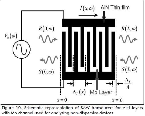
Taking SAW configuration from SEM results into account (Figure 10), coupling mode equations for AlN layers with Mo channel were derived and used for analysing non-dispersive SAW transducers with constant or arbitrary reflectivity weighting (Chen and Haus, 1985). The effects of propagation loss, electrode reflection, electrical transduction, acoustic reception, thin film loss and distributed finger capacitance have been included in the formulations. Some coupling of mode parameters become frequency-dependent for a dispersive layered SAW filter due to phase speed dispersion and had to be modified accordingly. Coupling mode equations governing SAW mode amplitudes R(x,ω), S(x,ω) propagating in ±x directions (Figure 8) can be arranged in a concise form for a uniform transducer, as follows (Chen and Haus, 1985; Chen et al., 2004):

where ΔT was transduction wavelength, V0 the voltage across the IDT, I current flow into the bus bar, k0= 2π/ΔT the transducer’s synchronous wavenumber.
Coordinates x = 0 and x = L were located at ΔT/4 distance away from the centre of the first and last IDT finger in the Mo/AlN/Si SAW configuration (Figure 10). Coupling mode equation parameters in this formulation were substrate Rayleigh wave speed, vR, transduction coefficient, α, AlN thin film resistance in one transduction period, RF, Mo inter-digital capacitance in one transduction period, CF, reflection parameter, K, and propagation loss per unit length, γ. It is worth noting that one transduction period consisted of two electrodes (Chen et al., 2004).
Mo/AlN SAW device frequency response
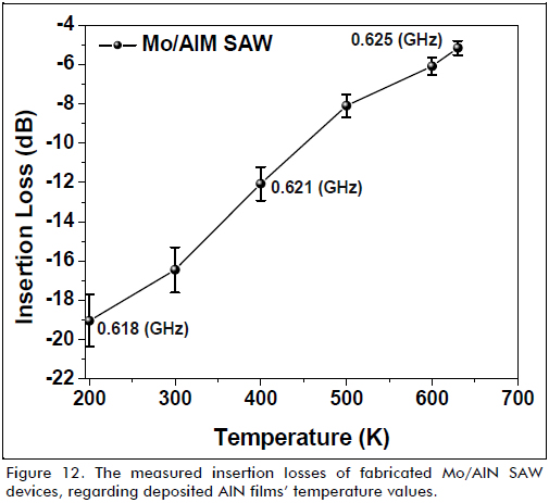
Frequency response characteristics of Mo/AlN SAW devices fabricated using differing deposition conditions, such as 200 K, 400 K and 630 K, were measured (Figure 11a–c). As can be clearly seen by comparing the wide-frequency scan spectra of the three devices (plotted in the inserts of Figure 11c), the centre frequency was shifted from around 0.618 GHz (Figure 11a) to higher frequencies of 0.621 GHz (Figure 11b) and 0.625 GHz (Figure 11c) by using the AlN buffer layers. This indicated that the AlN buffer layer could be used as high phase-speed substrate when manufacturing high-frequency SAW devices, as with Mo. Figure 11 shows that insertion loss became reduced by using different AlN buffer deposition temperatures. Insertion loss was measured for all fabricated SAW devices to examine insertion loss dependence on AlN-buffer deposition in more detail.

The results are plotted in Figure 12 regarding AlN film temperature deposition; estimated quantitative values are listed in Figure 11. Figure 12 shows that insertion loss for SAW devices fabricated using the sputtered-AlN buffer with Mo channel was exactly correlated to the corresponding temperatures for all AlN films. This could be identified by comparing the results obtained from the device with AlN films deposited on Si substrate. Temperature deposition for the above devices increased systematically, as already shown in Figure 12. The device with AlN deposited at 630 K revealed relatively large insertion loss in relation to frequency value (0.625 GHz). This may have been attributed to relatively low surface roughness (90 nm) of the AlN film used in Mo/AlN devices considering that AlN film surface roughness may have also been affected by AlN buffer layer surface morphology and deposition temperature (Jun-Phil Jung et al., 2004). Figure 12 confirms that frequency response characteristics (insertion loss) could be affected by reduced oxygen concentration, reduced grain size, roughness and decreased reflectance of AlN films together with increased colour purity and dominant wavelength. AlN buffer properties may have strongly governed the characteristics of a SAW device using the Mo/AlN system.
Determining Mo/AlN SAW devices’ acoustic wave speed
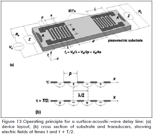
A basic SAW device (known as a delay line) is shown in Figure 13a. A piezoelectric substrate had a polished upper surface on which two IDTs were deposited using photolithographic methods. The left-hand input transducer was connected via fine bonded leads to the electricity source (Vs) through an electrical matching network (Z) and source resistance (Rs). The right-hand output transducer drove the load (RL), usually 50 ohms, through another electrical matching network (Z). Advances in computer modelling have led to the development of 50-ohm IDT designs which do not require external electrical matching networks. Resonance frequency and acoustic wave speed could thus be explained according to Eq. (5) (Branch et al., 2004).

where resonance frequency (f0) was governed by Rayleigh wave speed (VR) on the piezoelectric substrate, wave length (λ) and electrode width (a) of a single finger. SAW device wave speed depended on piezoelectric crystal properties and its crystallographic orientation (Hashimoto and Yamaguchi, 2001).
Mo/AlN SAW devices used inter-digital transducers (IDTs) fabricated onto a substrate to generate Rayleigh waves. The Rayleigh mode SAW had two particle displacement components in the sagittal plane. Surface particles moved in elliptical paths having a surface normal component and surface parallel component. The surface parallel component was parallel to the direction of propagation; the electromagnetic field associated with the acoustic wave travelled in the same direction. Wave speed was determined by the substrate material and the cut. These devices’ appearance was similar to that of Rayleigh SAW devices, but a thin solid film or grating was added to prevent wave diffraction into the bulk. Operating frequency was determined by IDT finger spacing and the wave speed for the particular substrate material. An example of piezoelectric behaviour is Si substrate deposited with AlN where the dominant acoustic wave propagating on 40°-rotated Y-cut, X propagating AlN/Si would be a shear horizontal surface mode. Acoustic wave (AW) propagation was not severely attenuated when the surface was loaded with a liquid, as with Rayleigh SAW-based devices (Kondoh and Shiokawa et al., 1993; Kondohand Shiokawa, 1995).
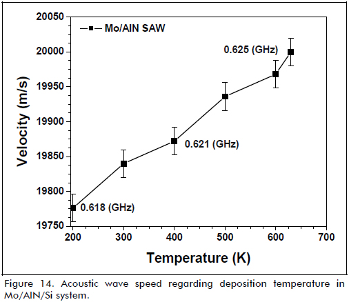
Rayleigh wave phase speed in Mo/AlN sample was simply calculated from Eq (5), and shown in Figure 14. The Rayleigh mode peak frequencies for all films showed deposition temperature-dependence. Rayleigh mode reflected signal in AlN films deposited at the highest temperature (630 K) was observed to be much stronger than that of AlN films deposited at lowest temperatures (200 K) and the phase speed of AlN films deposited at 630 K was much higher. The measured resonant frequencies for Rayleigh mode waves for The Mo/AlN SAW devices ranged from 618 MHz to 625 MHz corresponding to 19,776 m/s to 20,000 m/s phase speed, indicating good repeatability and reproducibility. The substrate’s lower deposition temperature caused perturbation of the acoustic speed which was related to a change in oscillator circuit frequency.
Conclusions
Temperature deposition was varied from 200 C to 630 C to analyse its effect on the films optical and morphological properties. X-ray photoelectron spectroscopy (XPS) confirmed binary film formation. The study revealed that temperature deposition had a marked influence on AlN films’ chemical and physical nature (oxygen concentration, grain size and roughness).
SAW propagation speed was strongly dependent on deposition conditions, Rayleigh mode and could be obtained with an h/λ ratio larger than 0.15. Reflection signal amplitude and phase and Rayleigh wave speed were increased leading to increased deposition temperature. An inter-digital structure having an Mo circuit on AlN films acting like an insulator was designed which could be used as a surface acoustic wave (SAW) device.
Acknowledgements
This work was financed by “El patrimonio Autónomo Fondo Nacional de Financiamiento para la Ciencia, la Tecnología y la Innovación, Francisco José de Caldas” contract RC-No. 275-2011 with Center of Excellence for Novel Materials (CENM). The authors would like to acknowledge Universitat de Barcelona’s Serveis Científico-Técnics for XPS, SEM and optical analysis.
References
Bass, M., Van Stryland, E. W., Handbook of Optics, Vol. 2: Devices, Measurements, and Properties., 2nd Ed., McGraw-Hill, 1994.
Bechmann, R., The piezo-optic and electro-optic constants of zincblende., Journal of Physics and Chemistry of Solids, Vol. 16, No. 1–2, Nov., 1960, pp. 100-101.
Branch, D. W., Brozik, S. M., Low-level detection of a Bacillus anthracis simulant using Love-wave biosensors on 36°YX LiTaO3., Biosensors and Bioelectronics, Vol. 19, No. 8, Mar., 2004, pp. 849–859.
Brien, V., Pigeat, P., Correlation between the oxygen content and the morphology of AlN films grown by r.f. magnetron sputtering., Journal of Crystal Growth, Vol. 310, No.16, Aug., 2008, pp. 3890-3895.
Caicedo, J. C., Zambrano, G., Aperador, W., Escobar-Alarcon, L., Camps, E., Mechanical and electrochemical characterization of vanadium nitride (VN) thin films., Applied Surface Science, Vol. 258, No. 1, Oct., 2011, pp. 312-320.
Chen, D. P., Haus, H. A., Analysis of metal-strip SAW gratings and transducers., IEEE Transactions. Sonics Ultrason, Vol. SU-32, 1985, pp. 395-408.
Chen, Y. -Y., Wu, T. -T., Chou, T. -T., Analysis of the frequency response of a dispersive IDT/ZnO/sapphire SAW filter using effective permittivity and the coupling of modes model., Journal of Physics D: Applied Physics, Vol. 37, No. 1, Jan., 2004, pp. 120–127.
Christensen, N. E., Gorczyca, I., Optical and structural properties of III-V nitrides under pressure., Volumes 47 – 66., Vol. 50, No. 7, 1994, pp. 4397-4415.
Clement, M., Vergara, L., Sangrador, J., Iborra, E., Sanz-Hervás, A., SAW characteristics of AlN films sputtered on silicon substrates., Ultrasonics, Vol. 42, No. 1–9, April, 2004, pp. 403-407.
Hashimoto, K. -Y., Yamaguchi, M., Excitation and propagation of shear-horizontal-type surface and bulk acoustic waves., Ultrasonics, Ferroelectrics and Frequency Control, Vol. 48, No. 5, Sep., 2001, pp. 1181–1188.
Hoummady, M., Campitelli, A., Acoustic wave sensors: design, sensing mechanisms and applications., Smart Materials and Structures, Vol. 6, No. 6, Dec., 1997, pp. 647-657.
Hoummady, M., Hauden, D., Acoustic wave thermal sensitivity: temperature sensors and temperature compensation in microsensors., Sensors and Actuators A: Physical, Vol. 45, No. 2, Nov., 1994, pp.167-172.
Hughes, J. L. P., Wang, Y., Sipe, J. E., Calculation of linear and second-order optical response in wurtziteGaN and AlN., Physical Review B: Volumes 67 – 86., Vol. 55, No. 20., 1997., pp. 13630-13640.
Jiang, L. F., Shen, W. Z., Ogawa, H., Guo, Q. X., Temperature dependence of the optical properties in hexagonal AlN., J. Appl. Phys., Vol. 94, 2003, pp. 5704.
Jung, J. -P., Lee, J. -B., Kim, J. -S., Park, J. -S., Fabrication and characterization of high frequency SAW device with IDT/ZnO/AlN/Si configuration: role of AlN buffer., Thin Solid Films, Vol. 447–448, Jan., 2004, pp. 605–609.
Kondoh, J., Shiokawa Commun S., A liquid sensor based on a shear horizontal saw device., Electronics and Communications in Japan (Part II: Electronics), Vol. 76, No. 2, Jun., 1993, pp. 69–82.
Kondoh, J., Shiokawa, S., Liquid identification using SH-SAW sensors., Solid-State Sensors and Actuators, 1995 and Eurosensors IX. Transducers '95. The 8th International Conference on Stockholm, Vol. 2, Jun., 1995, pp. 716–19.
Mahmood, A. M., Machorro, R., Heiras, J., Catrillon, F. F., Farias, M. H., Andrade, E., Optical and surface analysis of DC-reactive sputtered AlN films., Diamond and Releated Materials, Vol. 12, No.8, Jan., 2003, pp. 1315-1321.
Men, C., Lin, C., A comparison of pulsed-laser-deposited and ion-beam-enhanced-deposited AlN thin films for SOI application., Materials Science and Engineering: B, Vol. 133, No. 1–3, Aug., 2006, pp. 124-128.
Mcleod, H. A., Thin-film optical filters., CRC Press, 2001, pp. 158-159.
Niyomsoan, S., Grant, W., Olson, D. L., Mishra, B., Variation of color in titanium and zirconium nitride decorative thin films., Thin Solid Films, Vol. 415, No. 1, Aug., 2002, pp. 187-194.
Raole, P. M., Mukherjee, S., John, P. I., X-ray photoelectron spectroscopic study of plasma source nitrogen ion implantation in single crystal natural diamond., Diamond and Related Materials, Vol. 14, No. 3-7, Mar., 2005, pp. 482-485.
Ristoscu, C., Ducu, C., Socol, G., Craciunoiu, F., Mihailescu, I. N., Structural and optical characterization of AlN films grown by pulsed laser deposition., Applied Surface Science, Vol. 248, No. 1–4, July, 2005, pp. 411-415.
Rosenberger, L., Baird, R., McCullen, E., Auner, G., Shreve, G., XPS analysis of aluminum nitride films deposited by plasma source molecular beam epitaxye., Surface and Interface Analysis, Vol. 40, No. 9, Sept., 2008, pp. 1254-1261.
Taylor, J. A., Rabalais, J. W., Reaction of N2+ beams with aluminum surfaces., Journal of Chemical Physics, Vol. 75, No. 4, 1981.
Wang, P. W., Sui, S., Wang, W., Durrer, W., Aluminum nitride and alumina composite film fabricated by DC plasma processes., Thin Solid Films, Vol. 295, No. 1, Feb., 1997, pp. 142-146.
Yamashita, H., Fukui, K., Misawa, S., Yoshida, S., Optical properties of AlN epitaxial thin films in the vacuum ultraviolet region., J. Appl. Phys., Vol. 50, 1979, pp. 896.
Zayats, N. S., Boiko, V. G., Gentsar, P. A., Litvin, O. S., Papusha, V. P., Sopinskii, N. V., Optical studies of AlN/n-Si(100) films obtained by the method of high-frequency magnetron sputtering., Semiconductor, Vol. 42, No. 2, 2008, pp. 195-198.
Zhuang, C., Zhao, J., Jia, F., Guan, C., Wu, Z., Bai, Y., Jiang, X., Tuning bond contents in B–C–N films via temperature and bias voltage within RF magnetron sputtering., Surface and Coatings Technology, Vol. 204, No. 5, Dec., 2009, pp. 713-717.
References
Bass, M., Van Stryland, E. W., Handbook of Optics, Vol. 2: Devices, Measurements, and Properties., 2nd Ed., McGraw-Hill, 1994.
Bechmann, R., The piezo-optic and electro-optic constants of zincblende., Journal of Physics and Chemistry of Solids, Vol. 16, No. 1–2, Nov., 1960, pp. 100-101. DOI: https://doi.org/10.1016/0022-3697(60)90078-0
Branch, D. W., Brozik, S. M., Low-level detection of a Bacillus anthracis simulant using Love-wave biosensors on 36°YX LiTaO3., Biosensors and Bioelectronics, Vol. 19, No. 8, Mar., 2004, pp. 849–859. DOI: https://doi.org/10.1016/j.bios.2003.08.020
Brien, V., Pigeat, P., Correlation between the oxygen content and the morphology of AlN films grown by r.f. magnetron sputtering., Journal of Crystal Growth, Vol. 310, No.16, Aug., 2008, pp. 3890-3895. DOI: https://doi.org/10.1016/j.jcrysgro.2008.06.021
Caicedo, J. C., Zambrano, G., Aperador, W., Escobar-Alarcon, L., Camps, E., Mechanical and electrochemical characterization of vanadium nitride (VN) thin films., Applied Surface Science, Vol. 258, No. 1, Oct., 2011, pp. 312-320. DOI: https://doi.org/10.1016/j.apsusc.2011.08.057
Chen, D. P., Haus, H. A., Analysis of metal-strip SAW gratings and transducers., IEEE Transactions. Sonics Ultrason, Vol. SU-32, 1985, pp. 395-408. DOI: https://doi.org/10.1109/T-SU.1985.31609
Chen, Y. -Y., Wu, T. -T., Chou, T. -T., Analysis of the frequency response of a dispersive IDT/ZnO/sapphire SAW filter using effective permittivity and the coupling of modes model., Journal of Physics D: Applied Physics, Vol. 37, No. 1, Jan., 2004, pp. 120–127. DOI: https://doi.org/10.1088/0022-3727/37/1/020
Christensen, N. E., Gorczyca, I., Optical and structural properties of III-V nitrides under pressure., Volumes 47 – 66., Vol. 50, No. 7, 1994, pp. 4397-4415. DOI: https://doi.org/10.1103/PhysRevB.50.4397
Clement, M., Vergara, L., Sangrador, J., Iborra, E., Sanz-Hervás, A., SAW characteristics of AlN films sputtered on silicon substrates., Ultrasonics, Vol. 42, No. 1–9, April, 2004, pp. 403-407. DOI: https://doi.org/10.1016/j.ultras.2004.01.034
Hashimoto, K. -Y., Yamaguchi, M., Excitation and propagation of shear-horizontal-type surface and bulk acoustic waves., Ultrasonics, Ferroelectrics and Frequency Control, Vol. 48, No. 5, Sep., 2001, pp. 1181–1188. DOI: https://doi.org/10.1109/58.949731
Hoummady, M., Campitelli, A., Acoustic wave sensors: design, sensing mechanisms and applications., Smart Materials and Structures, Vol. 6, No. 6, Dec., 1997, pp. 647-657. DOI: https://doi.org/10.1088/0964-1726/6/6/001
Hoummady, M., Hauden, D., Acoustic wave thermal sensitivity: temperature sensors and temperature compensation in microsensors., Sensors and Actuators A: Physical, Vol. 45, No. 2, Nov., 1994, pp.167-172. DOI: https://doi.org/10.1016/0924-4247(94)00843-4
Hughes, J. L. P., Wang, Y., Sipe, J. E., Calculation of linear and second-order optical response in wurtziteGaN and AlN., Physical Review B: Volumes 67 – 86., Vol. 55, No. 20., 1997., pp. 13630-13640. DOI: https://doi.org/10.1103/PhysRevB.55.13630
Jiang, L. F., Shen, W. Z., Ogawa, H., Guo, Q. X., Temperature dependence of the optical properties in hexagonal AlN., J. Appl. Phys., Vol. 94, 2003, pp. 5704. DOI: https://doi.org/10.1063/1.1616988
Jung, J. -P., Lee, J. -B., Kim, J. -S., Park, J. -S., Fabrication and characterization of high frequency SAW device with IDT/ZnO/AlN/Si configuration: role of AlN buffer., Thin Solid Films, Vol. 447–448, Jan., 2004, pp. 605–609. DOI: https://doi.org/10.1016/j.tsf.2003.07.022
Kondoh, J., Shiokawa Commun S., A liquid sensor based on a shear horizontal saw device., Electronics and Communications in Japan (Part II: Electronics), Vol. 76, No. 2, Jun., 1993, pp. 69–82. DOI: https://doi.org/10.1002/ecjb.4420760208
Kondoh, J., Shiokawa, S., Liquid identification using SH-SAW sensors., Solid-State Sensors and Actuators, 1995 and Eurosensors IX. Transducers '95. The 8th International Conference on Stockholm, Vol. 2, Jun., 1995, pp. 716–19.
Mahmood, A. M., Machorro, R., Heiras, J., Catrillon, F. F., Farias, M. H., Andrade, E., Optical and surface analysis of DC-reactive sputtered AlN films., Diamond and Releated Materials, Vol. 12, No.8, Jan., 2003, pp. 1315-1321. DOI: https://doi.org/10.1016/S0925-9635(03)00076-1
Men, C., Lin, C., A comparison of pulsed-laser-deposited and ion-beam-enhanced-deposited AlN thin films for SOI application., Materials Science and Engineering: B, Vol. 133, No. 1–3, Aug., 2006, pp. 124-128. DOI: https://doi.org/10.1016/j.mseb.2006.06.016
McLeod, H. A., Thin-film optical filters., CRC Press, 2001, pp. 158-159. DOI: https://doi.org/10.1201/9781420033236
Niyomsoan, S., Grant, W., Olson, D. L., Mishra, B., Variation of color in titanium and zirconium nitride decorative thin films., Thin Solid Films, Vol. 415, No. 1, Aug., 2002, pp. 187-194. DOI: https://doi.org/10.1016/S0040-6090(02)00530-8
Raole, P. M., Mukherjee, S., John, P. I., X-ray photoelectron spectroscopic study of plasma source nitrogen ion implantation in single crystal natural diamond., Diamond and Related Materials, Vol. 14, No. 3-7, Mar., 2005, pp. 482-485. DOI: https://doi.org/10.1016/j.diamond.2004.11.009
Ristoscu, C., Ducu, C., Socol, G., Craciunoiu, F., Mihailescu, I. N., Structural and optical characterization of AlN films grown by pulsed laser deposition., Applied Surface Science, Vol. 248, No. 1–4, July, 2005, pp. 411-415. DOI: https://doi.org/10.1016/j.apsusc.2005.03.112
Rosenberger, L., Baird, R., McCullen, E., Auner, G., Shreve, G., XPS analysis of aluminum nitride films deposited by plasma source molecular beam epitaxye., Surface and Interface Analysis, Vol. 40, No. 9, Sept., 2008, pp. 1254-1261. DOI: https://doi.org/10.1002/sia.2874
Taylor, J. A., Rabalais, J. W., Reaction of N2+ beams with aluminum surfaces., Journal of Chemical Physics, Vol. 75, No. 4, 1981. DOI: https://doi.org/10.1063/1.442251
Wang, P. W., Sui, S., Wang, W., Durrer, W., Aluminum nitride and alumina composite film fabricated by DC plasma processes., Thin Solid Films, Vol. 295, No. 1, Feb., 1997, pp. 142-146. DOI: https://doi.org/10.1016/S0040-6090(96)09270-X
Yamashita, H., Fukui, K., Misawa, S., Yoshida, S., Optical properties of AlN epitaxial thin films in the vacuum ultraviolet region., J. Appl. Phys., Vol. 50, 1979, pp. 896. DOI: https://doi.org/10.1063/1.326007
Zayats, N. S., Boiko, V. G., Gentsar, P. A., Litvin, O. S., Papusha, V. P., Sopinskii, N. V., Optical studies of AlN/n-Si(100) films obtained by the method of high-frequency magnetron sputtering., Semiconductor, Vol. 42, No. 2, 2008, pp. 195-198. DOI: https://doi.org/10.1134/S1063782608020139
Zhuang, C., Zhao, J., Jia, F., Guan, C., Wu, Z., Bai, Y., Jiang, X., Tuning bond contents in B–C–N films via temperature and bias voltage within RF magnetron sputtering., Surface and Coatings Technology, Vol. 204, No. 5, Dec., 2009, pp. 713-717. DOI: https://doi.org/10.1016/j.surfcoat.2009.09.031
How to Cite
APA
ACM
ACS
ABNT
Chicago
Harvard
IEEE
MLA
Turabian
Vancouver
Download Citation
CrossRef Cited-by
1. Jiin-Jyh Shyu, Chia-Wei Yang. (2017). Improvement of photoluminescence intensity of Ce-doped Y3Al5O12 phosphor by Si3N4 addition. Materials Chemistry and Physics, 193, p.339. https://doi.org/10.1016/j.matchemphys.2017.02.035.
2. Sea-Fue Wang, Kuo-Kwang Chao, Yi-Le Liao, Hsiao-Hsuan Hsu, Edward Yi Chang. (2024). Relations among composition, microstructure, and mechanical and dielectric properties from 1 MHz to 100 GHz of aluminum nitride substrates. Journal of Alloys and Compounds, 1005, p.176147. https://doi.org/10.1016/j.jallcom.2024.176147.
3. Guillaume Gommé, Adrien Cutivet, Boussairi Bouzazi, Abderrahim Rahim Boucherif, Tom MacElwee, Christophe Rodriguez, Meriem Bouchilaoun, Hubert Pelletier, Philippe-Olivier Provost, Hassan Maher, Richard Ares. (2020). AlN grown by CBE for power device applications. AIP Advances, 10(6) https://doi.org/10.1063/1.5142615.
4. Shiqi Zhu, Xiyan Zhang, Biao Li, Liqun Cheng, He Tang, Qingxi Li, Wenmin Zhang, Xiaoyun Mi, Liping Lu, Hongwei Liu. (2018). The effect of different Si4+ and N3− ratios on luminescent properties of Y2.85Al5-ySiyO12-(3x-y)/2Nx: Ce3+0.15 phosphors. Journal of Alloys and Compounds, 767, p.1102. https://doi.org/10.1016/j.jallcom.2018.07.189.
5. Mahshid Rashidi, Morteza Tamizifar, Seyyed Mohammad Ali Boutorabi. (2020). Characteristics of TiAlCN ceramic coatings prepared via pulsed-DC PACVD, part I: Influence of precursors’ ratio. Ceramics International, 46(2), p.1269. https://doi.org/10.1016/j.ceramint.2019.06.303.
Dimensions
PlumX
Article abstract page views
Downloads
License
Copyright (c) 2013 Julio Cesar Caicedo, Jaime Andrés Pérez Taborda, Willian Aperador Chaparro

This work is licensed under a Creative Commons Attribution 4.0 International License.
The authors or holders of the copyright for each article hereby confer exclusive, limited and free authorization on the Universidad Nacional de Colombia's journal Ingeniería e Investigación concerning the aforementioned article which, once it has been evaluated and approved, will be submitted for publication, in line with the following items:
1. The version which has been corrected according to the evaluators' suggestions will be remitted and it will be made clear whether the aforementioned article is an unedited document regarding which the rights to be authorized are held and total responsibility will be assumed by the authors for the content of the work being submitted to Ingeniería e Investigación, the Universidad Nacional de Colombia and third-parties;
2. The authorization conferred on the journal will come into force from the date on which it is included in the respective volume and issue of Ingeniería e Investigación in the Open Journal Systems and on the journal's main page (https://revistas.unal.edu.co/index.php/ingeinv), as well as in different databases and indices in which the publication is indexed;
3. The authors authorize the Universidad Nacional de Colombia's journal Ingeniería e Investigación to publish the document in whatever required format (printed, digital, electronic or whatsoever known or yet to be discovered form) and authorize Ingeniería e Investigación to include the work in any indices and/or search engines deemed necessary for promoting its diffusion;
4. The authors accept that such authorization is given free of charge and they, therefore, waive any right to receive remuneration from the publication, distribution, public communication and any use whatsoever referred to in the terms of this authorization.


