Published

2024-05-29

Channel Operating Margin Exploration as a Complementary Transceiver Circuit Design Tool for 25 Gbps PAM4 Serial Links

Exploración del margen operativo del canal como herramienta complementaria para el diseño de circuitos transceptores con enlaces seriales PAM4 de 25 Gbps

DOI:

https://doi.org/10.15446/ing.investig.106310

Keywords:

COM, Equalizers, IEEE 802.3ck, eye diagram, single-bit response (en)
COM, ecualizadores, IEEE 802.3ck, diagrama de ojo, respuesta a único bit (es)

Downloads

Authors

The design of high-speed serial links continues to attract the attention of the electronics industry due to the steady development of different telecommunications standards, generating a constantly growing data rate and new modulation schemes. However, conventional certification metrics can lead to sub-optimal transmit (Tx) and receive (Rx) circuit designs. Therefore, the Ethernet standard IEEE 802.3bj introduced a more effective evaluation method called channel operating margin (COM) to explore the design space at an early stage. Although the advantages of COM have been discussed in the literature and only a few works explore its potential as a backplane design tool, there are no reports on the use of COM as a complementary design tool for transceiver circuits. This work studies the use of COM as a complementary tool for transceiver design. COM performance is evaluated for four 100GBASE-KP4 backplanes and different equalization architectures. The impact of the metric and the challenges associated with incorporating new equalization structures into the COM flow are discussed. The results reveal a conventional Tx-Rx architecture that exceeds the COM threshold and an alternative one that improves the opening of the eye diagram but does not exceed the threshold.

El diseño de enlaces seriales de alta velocidad continúa atrayendo la atención de la industria electrónica debido al desarrollo constante de diferentes estándares de telecomunicaciones, generando una tasa de datos en constante crecimiento y nuevos esquemas de modulación. Sin embargo, las métricas de certificación convencionales pueden llevar a diseños de circuitos de transmisión (Tx) y recepción (Rx) subóptimos. Por lo tanto, el estándar Ethernet IEEE 802.3bj introdujo un método de evaluación más efectivo llamado margen de operación del canal (COM, por sus siglas en inglés) para explorar el espacio de diseño en una etapa temprana. Aunque las ventajas de COM han sido discutidas en la literatura y solo unos pocos trabajos exploran su potencial como una herramienta de diseño de backplane, no hay informes sobre el uso de COM como una herramienta de diseño complementaria para circuitos transceptores. Este trabajo estudia el uso de COM como una herramienta complementaria para el diseño de transceptores. El rendimiento de COM se evalúa para cuatro backplanes 100GBASE-KP4 y diferentes arquitecturas de ecualización. Se discuten el impacto de la métrica y los desafíos asociados a la incorporación de nuevas estructuras de ecualización en el flujo de COM. Los resultados revelan una arquitectura Tx-Rx convencional que supera el umbral de COM y una alternativa que mejora la apertura del diagrama de ojo pero no supera el umbral de COM.

Recibido: 1 de mayo de 2023; Aceptado: 27 de febrero de 2024

Abstract

The design of high-speed serial links continues to attract the attention of the electronics industry due to the steady development of different telecommunications standards, generating a constantly growing data rate and new modulation schemes. However, conventional certification metrics can lead to sub-optimal transmit (Tx) and receive (Rx) circuit designs. Therefore, the Ethernet standard IEEE 802.3bj introduced a more effective evaluation method called channel operating margin (COM) to explore the design space at an early stage. Although the advantages of COM have been discussed in the literature and only a few works explore its potential as a backplane design tool, there are no reports on the use of COM as a complementary design tool for transceiver circuits. This work studies the use of COM as a complementary tool for transceiver design. COM performance is evaluated for four 100GBASE-KP4 backplanes and different equalization architectures. The impact of the metric and the challenges associated with incorporating new equalization structures into the COM flow are discussed. The results reveal a conventional Tx-Rx architecture that exceeds the COM threshold and an alternative one that improves the opening of the eye diagram but does not exceed the threshold.

Keywords

COM, equalizers, IEEE 802.3ck, eye diagram, single-bit response.

Resumen

El diseño de enlaces seriales de alta velocidad continúa atrayendo la atención de la industria electrónica debido al desarrollo constante de diferentes estándares de telecomunicaciones, generando una tasa de datos en constante crecimiento y nuevos esquemas de modulación. Sin embargo, las métricas de certificación convencionales pueden llevar a diseños de circuitos de transmisión (Tx) y recepción (Rx) subóptimos. Por lo tanto, el estándar Ethernet IEEE 802.3bj introdujo un método de evaluación más efectivo llamado margen de operación del canal (COM, por sus siglas en inglés) para explorar el espacio de diseño en una etapa temprana. Aunque las ventajas de COM han sido discutidas en la literatura y solo unos pocos trabajos exploran su potencial como una herramienta de diseño de backplane, no hay informes sobre el uso de COM como una herramienta de diseño complementaria para circuitos transceptores. Este trabajo estudia el uso de COM como una herramienta complementaria para el diseño de transceptores. El rendimiento de COM se evalúa para cuatro backplanes 100GBASE-KP4 y diferentes arquitecturas de ecualización. Se discuten el impacto de la métrica y los desafíos asociados a la incorporación de nuevas estructuras de ecualización en el flujo de COM. Los resultados revelan una arquitectura Tx-Rx convencional que supera el umbral de COM y una alternativa que mejora la apertura del diagrama de ojo pero no supera el umbral de COM.

Palabras clave

COM, ecualizadores, IEEE 802.3ck, diagrama de ojo, respuesta a único bit.

Introduction

Many high-speed serial links employ SerDes systems for transmission speeds of up to 112 Gb/s (Champion and Tracy, 2019). However, for rates exceeding 25 Gb/s, strict transceiver design is necessary to compensate for noise and crosstalk, ensuring compliance with certification metrics (Dong et al., 2014). Design parameters within the metric (Figure 1) must be met for each transmission speed. Evaluating parameters individually leads to performance misinterpretation, and inaccurate channel loss estimation affects transceiver circuit design (Filip, 2018).

The IEEE 802.3bj Ethernet standard introduced channel operating margin (COM) as a global certification metric for high-speed serial channels (IEEE, 2014). COM simplifies evaluation by measuring a single signal-to-noise ratio, encompassing the entire SerDes system. It aims to address channel performance ambiguities and facilitate trade-off analysis, potentially reducing transceiver complexity. However, COM documentation is limited. Works such as those by de Paulis et al. (2020), de Paulis et al. (2022), and Gore and Mellitz (2014) explore the use of COM oriented to backplanes design, with the absence of any report that uses COM as a complementary tool for transceiver architecture design.

Our work evaluates the feasibility of using COM as a transceiver design mechanism, addressing compliance issues with traditional strategies. We focus on Tx/Rx modeling within the COM validation metric. Modifications to the COM flow include incorporating new receiver-side equalization architectures. Specifically, decision feedback equalizer (DFE) architectures are studied using infinite impulse response (IIR) taps instead of discrete taps. Previous studies have demonstrated the advantages of DFE with IIR filters in terms of power consumption and equalization efficiency (Shahramian and Chan Carusone, 2015; Chen et al., 2017; Elhadidy and Palermo, 2013; Kim et al., 2009; Shahramian et al., 2016). DFE with IIR filters effectively cancels inter-symbol interference (ISI) with low circuit complexity. However, implementing DFE IIR within the COM computation flow introduces certain drawbacks, which are thoroughly discussed in this research.

The performance of various equalization architectures is evaluated using four 50 Gb/s channels from different companies, based on the parameters and specifications of the IEEE 802.3ck standard (Heck and Intel, 2018; Mellitz et al., 2018; Palkert and Molex, 2020). We discuss the performance of COM with different transceivers, identifying the one with the minimal complexity that achieves a final COM value greater than 3 dB for all cables. Additionally, we provide recommendations on using COM as a design mechanism.

This work explains COM and its impact on transceiver architecture, describing the utilization of COM as a tool for exploring transceiver architecture, and summarizes the COM results obtained for different equalization architectures. Additionally, it discusses considerations for incorporating different DFE architectures into the COM algorithm, presenting the results for different architecture variations. Finally, the main conclusions of this work are stated.

Evolution of validation metrics according to the data rate

Figure 1.: Evolution of validation metrics according to the data rate

Source: Authors

Channel operating margin (COM)

COM is a mathematical algorithm that determines a figure of merit (FoM) in decibels. The FoM is a signal-to-noise ratio (SNR) that compares the sampled signal against the total noise contribution. COM results offer valuable information regarding transmission quality for a specific transmission system (Tx-channel-Rx). For channels exceeding 25 Gb/s, the standard requires the SNR to exceed the 3 dB threshold for proper system functionality. As a time-domain metric, COM can also analyze interconnected systems, pinpointing strengths and weaknesses in Tx/Rx design. It serves as a communication bridge between signal integrity and SerDes designers.

Description and limitations of the COM algorithm

COM evaluates SerDes system performance under different conditions: transceiver circuit complexity, signal modulation, several channel impairments, and others, aiming to reduce the circuit design complexity. The user can import the s-parameter of the channel (these s-parameters can be downloaded from the repository of the 802.3ck IEEE standard) and the number of taps for the feed-forward equalizer (FFE) and DFE or gain for the continuous-time linear equalizer (CTLE).

COM transceiver architecture

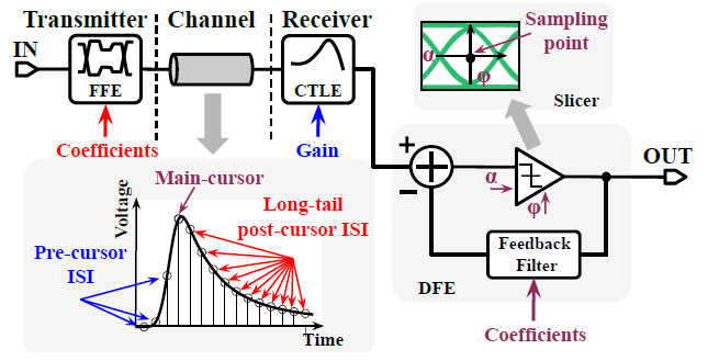
The COM transceiver topology includes a FFE on Tx and a CTLE along with a DFE on Rx. These equalizers mitigate ISI. The FFE primarily reduces pre-cursor ISI, while the CTLE and DFE reduce post-cursor ISI.

The COM FFE has three pre-cursors (c(-3), c(-2), c(-1)), one post-cursor (c(1)), and a main cursor (c(0)). The user defines the range for each tap. The weight of the main cursor (c(0)) is calculated using the following equation: c(0) = 1 - |c(1)| - |c(-1)| - |c(2)| - |c(-3)|.

After FFE, COM calculates the CTLE parameters. CTLE consists of two stages: the first stage (H_{CTLE}) for high frequencies has one zero around the Nyquist frequency (f_z) and two poles (f_{p1} and f_{p2}). The second stage (H_{CTLE2}) has a pole and a zero at the same frequency (f_{LF}), approximately 1/3 of the Nyquist frequency.

H_{CTLE}(f) = \frac{10^{\frac{g_{DCHF}}{10}} + j\frac{f}{f_z}}{(1 + j\frac{f}{f_{p1}})(1 + j\frac{f}{f_{p2}})} H_{CTLE2}(f) = \frac{10^{\frac{g_{DCLF}}{10}} + j\frac{f}{f_{LF}}}{(1 + j\frac{f}{f_{LF}})}

Figure 2 shows the behavior of the HF stage (Figure 2a) and the LF stage (Figure 2b) for the different DC gain values, marking f_{p2} for HF and f_{LF} for LF. The pole, zero, and DC gain parameters are defined externally by the user.

COM CTLE magnitude TF example. a) CTLE voltage gain for high frequencies; b) CTLE voltage gain for low frequencies.

Figure 2.: COM CTLE magnitude TF example. a) CTLE voltage gain for high frequencies; b) CTLE voltage gain for low frequencies.

Source: Authors

After CTLE, the next equalization stage is DFE. The COM DFE model is ideal and supports 1-35 post-cursor taps. The phase detector algorithm used in the CDR criterion is similar to that proposed by Mueller and Muller (1976), defining the sample point from the channel equalized single-bit-response (SBR).

Transceiver optimization cycle

To maximize the FoM, the algorithm exhaustively searches all possible combinations of the TxFFE, CTLE, and DFE parameters, evaluating a unique SBR for each combination.

FoM = 10\log_{10}\left(\frac{A_s^2}{\sigma_{Tx}^2 + \sigma_{ISI}^2 + \sigma_{IT}^2 + \sigma_{XT}^2 + \sigma_N^2}\right)

The numerator A_s corresponds to the value of the available signal, and the denominator parameters correspond to the noise contributions. The sum of denominator terms determines the amplitude of the noise interference.

The size of the COM exploration space depends on the number of parameters defined in each equalizer. For example, a transceiver architecture with two different values for HF DC gain, one value for LF DC gain, 3-FFE taps, and 3-DFE taps results in an eight-dimensional space that needs to be optimized.

Since COM was developed in the MATLAB sequential environment, to calculate the FoM, it implements a series of steps to optimize each parameter:

First, the algorithm evaluates the Equations 1 and 2 for the first values of the HF and the LF DC gain to determine the transfer function of the CTLE. Then, the algorithm sequentially computes the amplitude of each FFE tap (c(-3), c(-2), c(-1), c(1)). The amplitude of c(0) must meet the condition that c(0) = 1 - |c(1)| - |c(-1)| - |c(2)| - |c(-3)| > 0.5 to ensure that all transmitters support the FFE architecture. If c(0) does not reach the threshold, the algorithm selects another combination of amplitudes until c(0) exceeds 0.5. The FFE function is constructed and applied to the impulse response along with the CTLE transfer function to calculate the SBR for each channel. Next, COM estimates the sampling time, the value of the available signal A_s, and the amplitude of the DFE tap from the SBR of the THRU channel. A_s is calculated using Equation 4, where t_s is the sample point and R_{LM} is the level mismatch ratio. Additionally, COM computes an approximation of noise from a normal distribution of each noise contribution.

A_s = \frac{R_{LM} \cdot SBR(t_s)}{(level - 1)}

Finally, COM calculates the FoM using A_s and the noise approximation through Equation 3, where the noise approximation corresponds to the denominator and A_s to the numerator.

This process repeats for all possible combinations of the equalization parameters, obtaining a different FoM for each cycle. All FoM results are compared, selecting the best result and extracting the equalization parameters.

COM as transceiver exploration

SerDes architectures comprise a pre-emphasis on TX, usually an FFE, along with CTLE and DFE on Rx, as shown in Figure 3. Traditional transceiver design methodology causes transceiver circuit over-design or incorrect system validation due to excessive design margins (Filip, 2018). This section explores how to avoid these problems, specifically examining the feasibility of using the specification itself to evaluate the impact of different equalizer settings. This evaluation consists of obtaining different COM values by varying equalizer settings such as the FFE coefficients, the DC gain of the CTLE, or the DFE coefficients. In addition to the variation of the FFE, CTLE, and DFE parameters, we also explore the impact of adding a second CTLE in the cascade connection on the optimization loop. The testbench used to evaluate the equalization architecture (EQA) performance is composed of four different channels from different companies, as provided by standard IEEE 802.3ck.

Typical equalization scheme of a serial-link transceiver

Figure 3.: Typical equalization scheme of a serial-link transceiver

Source: Authors

COM exploration setup

To obtain the COM exploration space, we considered the conditions and parameters provided by the IEEE 802.3ck update, which are summarized in Table 1. The user can change the parameters defined in this Table. We can define the DC gain range of the HF stage (g_{DCHF}) and the LF stage (g_{DCLF}) for the CTLE, the number of activated taps for the FFE (from c(-3) to c(1)), as well as the amplitude range of each sample. Furthermore, with the N_b parameter, the user can activate up to 35-DFE taps. COM exploration space will be analyzed in two case studies: case study 1 corresponds to conventional equalization structures (FFE + CTLE + DFE), and case study 2 has an additional CTLE in its equalization structure.

Once the parameters are defined, the CTLE architecture is modified, adding an extra scale factor in Equation 1 as well as modifying the DC peaking gain from -3 to 3 dB (Figure 4). This change also applies to the additional CTLE used for case study 2.

CTLE DC peaking gain modification

Figure 4.: CTLE DC peaking gain modification

Source: Authors

The setup defined in Table 1 evaluates two different package length tests (z_p), one with a long package (length = 30 mm) and another one with a short package (length = 12 mm). Each package case results in a different COM value. The long package exhibits a lower COM due to more IL. Therefore, the reported results corresponded to a long package test. Additionally, Table 1 describes other important parameters, such as the signaling rate (f_b), the target detector error ratio (DER_0), and the level separation mismatch ratio (R_{LM}).

Table 1.: Simulation parameters setup

Source: Authors

Once COM exploration settings are defined, the four backplane channels from the IEEE 802.3ck study group (Heck and Intel, 2018; Mellitz et al., 2018; Palkert and Molex, 2020) are selected to test the EQAs' performance. The channel responses for channels Intel (Heck and Intel, 2018), Molex (Palkert and Molex, 2020), Samtec Op1, and Samtec Op2 (Mellitz et al., 2018) are shown in Figure 5. All channels have an insertion loss of approximately 28 dB@26 GHz (Figure 5a). Figure 5b shows that the unequalized SBRs are normalized and centered by unit interval (UI) at f_b = 53.125 Gb/s, highlighting the three sample moments: the pre-cursor in green, the cursor as a black line, and the post-cursor in pink. In Figure 5a, the first two pre-cursor samples have the highest ISI contribution, suggesting that at least two taps of the Tx FFE are needed. In addition, the samples after the cursor determine the CTLE gains and the amplitude of the DFE leads.

Table 2.: Characteristics of the test channel

Source: Authors

Test channel responses: a) insertion loss of all channels with an IL around 28 dB@26.56 GHz; b) SBR of the four backplane channels

Figure 5.: Test channel responses: a) insertion loss of all channels with an IL around 28 dB@26.56 GHz; b) SBR of the four backplane channels

Source: Authors

Table 2 summarizes the main characteristics of each channel. Highlighted in red, the Molex is the critical channel of the group, with the highest loss estimate (the highest insertion loss and the lowest effective return loss values). With this information, and using the traditional validation metric based on frequency limits, we can predict that the Molex channel might need a more complex transceiver circuit and perhaps report the lowest COM results relative to the other channels.

Simulations results and comparison

Figures 6 present four EQAs. The first EQA (Figure 6a) evaluates the impact of the variation of the FFE taps vs. the final value of the COM. This test performs a parametric sweep of the FFE taps, where 0 represents the absence of an FFE. The other three EQAs evaluate the impact of the variation of the DFE taps vs. the COM results via a parametric sweep of the DFE taps from 1 to 15 samples. The first two EQAs (6a and 6b) include all equalizers, while 6c and 6d do not contain one of the equalizers. The results show that, for all the cases that perform a parametric DFE sweep, COM saturation is achieved after a 3-tap DFE, suggesting that no more than 3-DFE taps are necessary. The minimal EQA reporting a COM result with an up to 3 dB margin is enclosed in a gray box (Figures 6a and 6b), where case 6a uses 5-FFE taps, the CTLE, and 1-DFE tap, and case 6b uses 3-FFE taps, the CTLE, and 3-DFE taps.

COM value for four common EQAs with a parametric sweep of TxFFE and DFE taps, including all contributions from the crosstalk channel. The complexity of the equalizer circuit increases from left to right on the x-axis.

Figure 6.: COM value for four common EQAs with a parametric sweep of TxFFE and DFE taps, including all contributions from the crosstalk channel. The complexity of the equalizer circuit increases from left to right on the x-axis.

Source: Authors

Similarly to case study 1, four different EQAs are selected for case study 2. However, we assumed that adding a second CTLE in the cascade connection might decrease the number of DFE taps. This variation of the CTLE architecture makes no modifications to the predefined CTLE parameters. Figure 7 shows the COM results for the four EQAs. The first three EQAs (7a, 7b, and 7c) perform a parametric sweep of the FFE taps, but case 7c does not use any CTLE, and case 7d exhibit COM saturation after 3-DFE taps, as in case study 1. Note that, although the COM results behave similarly to those of case study 1, the former minimum architecture comprises two equal CTLEs. In addition, as in case study 1, the COM value does not meet the threshold if one of the equalizers is removed.

COM values for four common EQAs with a parametric sweep of TxFFE and DFE taps, including all contributions from the crosstalk channel and two CTLEs. The complexity of the equalizer circuit increases from left to right on the x-axis.

Figure 7.: COM values for four common EQAs with a parametric sweep of TxFFE and DFE taps, including all contributions from the crosstalk channel and two CTLEs. The complexity of the equalizer circuit increases from left to right on the x-axis.

Source: Authors

In both case studies, the results confirm our initial hypothesis that the Molex channel requires a more complex transceiver circuit and yields the lowest COM results. Figures 6 and 7 demonstrate that, for all EQAs in both case studies, the COM results for the Molex channel resemble those obtained using the Samtec channels with the lowest estimated losses. This example highlights how COM can prevent the transceiver over-design resulting from a misinterpretation of channel losses using traditional validation metrics. Unlike validation metrics that drive transceiver design methodologies, COM can serve as a parallel design tool to validate design decisions and experimental EQAs, thus reducing chip over-design.

DFE IIR strategy in COM

Figure 8 shows the block diagram and the equalization process for a discrete 1-tap DFE applied 1/2 UI before and after each post-cursor. A DFE comprises a slicer that makes a symbol decision without amplifying the noise and a feedback loop with weighted derivation coefficients (H1, H2, through HN). Those coefficients are added to the input, canceling the post-cursor ISI. DFE implementations often employ up to ten feedback taps to achieve high-loss channel equalization. Unfortunately, the large number of feedback circuits used in a multi-tap DFE consumes significant power and chip area.

A discrete DFE architecture of N taps

Figure 8.: A discrete DFE architecture of N taps

Source: Authors

Some works (Shahramian and Chan Carusone, 2015; Chen et al., 2017; Elhadidy and Palermo, 2013; Kim et al., 2009; Shahramian et al., 2016) explore power reduction in DFE with multiple taps. These works propose employing IIR filters to create continuous-time taps, enabling the simultaneous cancellation of several post-cursor ISI taps and achieving a reduction in power consumption and circuit complexity. EQAs that utilize DFE with IIR taps demonstrate enhanced equalization efficiency for backplane channels (Elhadidy and Palermo, 2013).

This section reviews state-of-the-art DFE architectures with IIR filters and analyzes their impact on the COM algorithm. Furthermore, a discussion of COM results for various EQAs is presented.

DFE IIR prior art

Channels with high post-cursor ISI require multi-tap DFE, increasing chip area and power consumption. However, the ISI can be represented by a decreasing exponential in the SBR. Some studies present DFE architectures using IIR filters in the feedback loop, canceling multiple post-cursor samples with a single tap and reducing power and area consumption (Shahramian and Chan Carusone, 2015; Chen et al., 2017; Elhadidy and Palermo, 2013; Kim et al., 2009; Shahramian et al., 2016). Like a traditional DFE, IIR DFE cancels post-cursor ISI without noise amplification. Figure 9 shows the diagram of a DFE IIR with a single feedback loop that efficiently eliminates post-cursor ISI of up to three UI compared to a traditional discrete DFE.

A DFE IIR architecture

Figure 9.: A DFE IIR architecture

Source: Authors

Figure 10 compares three DFE architectures using IIR filters. The first two are pure DFE IIR architectures, while the third combines one discrete tap with two IIR filters. The DFE IIR architecture in Figure 10a compensates for up to two post-cursor samples with low complexity. However, one IIR filter is insufficient for complete post-cursor ISI elimination, as ISI is only partially eliminated after the third tap. The DFE with two IIR architectures in Figure 10b provides better equalization by covering fast and slow decaying ISI tails. However, implementing a DFE IIR can degrade signal integrity as the feedback loop delay increases.

Architectures for link DFE IIR feedback equalization: a) one IIR in the first tap; b) two IIRs in the first tap; c) one discrete tap and two IIRs in the second tap

Figure 10.: Architectures for link DFE IIR feedback equalization: a) one IIR in the first tap; b) two IIRs in the first tap; c) one discrete tap and two IIRs in the second tap

Source: Authors

As a solution to delay degradation, Shahramian and Chan Carusone (2015) propose a DFE architecture that combines one discrete-time tap with IIR filters, as depicted in Figure 10c. This architecture achieves a better fit for ISI because the first discrete tap decays faster than the other post-cursor samples. However, it is important to carefully select the number of implemented IIR filters to avoid excessive power and area consumption.

This study integrates two decision feedback equalizers into the COM algorithm (Figure 10), the first with 1-IIR and the other with 2-IIR.

Challenges of implementing DFE IIR in COM

Figure 11 compares different DFE architectures: Figure 11a shows a DFE with only IIR filters in the first tap, while Figure 11b combines a discrete branch with IIR filters. The two filters, VIIR1 and VIIR2, have two different time constants, one for the fast-decaying (VIIR1 in blue) and the other for the slow-decaying (VIIR2 in red).

Behavior of DFE architectures implemented in COM: a) DFE with 2IIR in the first taps; b) DFE with one discrete tap along with two IIRs in the second tap

Figure 11.: Behavior of DFE architectures implemented in COM: a) DFE with 2IIR in the first taps; b) DFE with one discrete tap along with two IIRs in the second tap

Source: Authors

To implement a DFE architecture with IIR filters in the COM algorithm, the impulse response of the filter was defined using Equation 5. This equation captures the decaying exponential behavior characteristic of the post-cursor ISI. The IIR filter is represented by two terms, the first term (0 \leq t \leq t1) models the increasing behavior of the impulse response in one UI. The second term captures the decreasing behavior of the post-cursor long-tail ISI. The constants RC and RC2 correspond to the increasing and decreasing time constants, while A and B represent the SBR values at t = 0 and t = t1, respectively.

V_{IIR}(t) = \left\{ \begin{array}{ll} A(1 - e^{-t/RC}) & 0 \leq t \leq t1 \\ B(e^{-t/RC2}) & t > t1 \end{array} \right.

Using Equation 5, the COM algorithm was modified regarding two key points:

- FoM maximization loop. In the FoM loop, we replaced the process of DFE coefficients calculation with Equation 5, operating only the post-cursor samples of the SBR. We also modified the computation of sigma ISI to consider the residual post-cursor taps from SBR after DFE IIR effects instead of the direct subtraction of traditional DFE taps to SBR.

- Total noise contribution. Once the FoM optimization process ends, the total noise contribution A_{ni} used for the COM calculation is estimated as was shown in the previous sections. Figure 12 presents the process of obtaining the ISI noise contribution with a DFE with one discrete tap. The DFE response in blue is applied to the SBR in gray, resulting in the residual response used to compute the total ISI noise. Nevertheless, the DFE implemented in COM includes floating DFE taps highlighted in gray, which add extra compensation for the other post-cursor samples. In addition to extra compensation, the cursor sample is eliminated to consider only the residual response after the complete equalization process. Due to the high impact of floating taps in the COM results (up to 1 dB difference, as presented in Figure 11), the COM results obtained with traditional discrete DFE are recalculated to properly compare the different new DFE architectures.

Residual response and COM results using a) DFE floating taps b) no DFE floating taps

Figure 12.: Residual response and COM results using a) DFE floating taps b) no DFE floating taps

Source: Authors

The results are classified into two different groups. Each group comprises four EQAs with a variation of the DFE architecture, along with an FFE with five taps (c(1), c(0), c(-1), c(-2), c(-3)) and a CTLE without peaking gain modifications. The first group includes a pure DFE IIR with up to two IIR filters on the first tap. The second group uses a DFE with one discrete tap along with one and two IIR filters in the second tap. The COM results were obtained by implementing the same testbench and the setup defined in Table 1. Additionally, we compared the results obtained with the different DFE modifications against an equivalent architecture that uses the traditional discrete DFE. However, in this section, the COM results are recalculated with a traditional DFE architecture due to, now the DFE does not include floating taps, causing a significant COM reduction regarding the previous results.

Simulation results

We selected twelve different EQA combinations and grouped them, as previously mentioned. The main objective of this Section is to determine the least complex solution in which COM achieves the margin. Figure 13a presents the impact of a pure DFE IIR along with different FFE and CTLE combinations vs. the final value of the COM. Since the IIRs are in the first tap, the COM results obtained from equivalent EQAs with a 1-tap DFE are presented in Figure 13b. The x-axis corresponds to different channel models, showing all the results for each channel.

COM performance of four different EQAs, including all crosstalk channel contributions: a) EQA with a DFE with one and two IIR taps; b) commonly used EQAs

Figure 13.: COM performance of four different EQAs, including all crosstalk channel contributions: a) EQA with a DFE with one and two IIR taps; b) commonly used EQAs

Source: Authors

It is relevant to note that, in Figure 13a, the EQA in green is the only one that uses two IIR filters. This consideration is since most of the long ISI tail is compensated by the CTLE, requiring a DFE with few taps. Therefore, for EQA with CTLE, the use of more than one IIR is unnecessary. This effect was evidenced in Figures 6 and 7, where the COM result showed saturation after 3-taps DFE for EQA including the CTLE.

DFE IIR response for different Intel SBRs: a) DFE with an IIR for a fast-decaying SBR; b) DFE with an IIR for a slow-decay SBR; c) DFE with two IIR fast IIR (blue) and slow IIR (red)

Figure 14.: DFE IIR response for different Intel SBRs: a) DFE with an IIR for a fast-decaying SBR; b) DFE with an IIR for a slow-decay SBR; c) DFE with two IIR fast IIR (blue) and slow IIR (red)

Source: Authors

Replacing a traditional DFE with a pure DFE yields an improvement in the COM value, particularly when EQAs have only two equalizers. However, the transceiver architecture that achieves a 3 dB COM is equally complex to the one discussed in the previous section. Moreover, none of the EQAs can compensate for the high losses of the Intel channel. Figure 14 illustrates the designed DFE IIR function, which perfectly fits the ISI of the SBR. In the case with two IIRs (Figure 14c), the DFE response corresponds to the sum of the fast-decaying and the slow-decaying IIRs, canceling up to six post-cursor taps.

In a second equalization experiment, we selected four different EQAs, combining a discrete tap with IIR taps in the DFE architecture. It has been demonstrated (Shahramian and Chan Carusone, 2015) that this combination achieves a better fit of ISI. Therefore, using this DFE architecture, the COM results might exceed the 3 dB threshold with just two equalizers.

COM performance of four different EQAs, including all crosstalk channel contributions: a) EQA with a DFE with one and two IIR taps; b) commonly used EQAs

Figure 15.: COM performance of four different EQAs, including all crosstalk channel contributions: a) EQA with a DFE with one and two IIR taps; b) commonly used EQAs

Source: Authors

By comparing the DFE responses in Figures 14 and 16, a perfect fit canceling more than six post-cursor taps can be observed in both cases. Still, similarly to the results presented in the previous chapter, only one of the equalization architectures surpasses the 3 dB COM threshold. In Figures 13 and 15, however, there is an improvement in the COM with the DFE IIR. By comparing the results obtained using the architecture with CTLE+DFE IIR and CTLE+1DFE in Figure 13, we observed an improvement of around 5 dB in the COM result using DFE IIR vs. that with the traditional DFE.

Discrete DFE and DFE IIR response for different Intel SBRs: a) DFE with one FIR tap and one IIR for a fast-decaying SBR; b) DFE with one FIR tap and one IIR for a slow decay SBR; c) DFE with one FIR tap and one IIR, fast IIR (red), and slow IIR (dotted red)

Figure 16.: Discrete DFE and DFE IIR response for different Intel SBRs: a) DFE with one FIR tap and one IIR for a fast-decaying SBR; b) DFE with one FIR tap and one IIR for a slow decay SBR; c) DFE with one FIR tap and one IIR, fast IIR (red), and slow IIR (dotted red)

Source: Authors

Figures 17 and 18 show the eye diagrams of the Intel channel equalized by different EQAs. While increasing the number of IIR filters in the DFE leads to a drastic improvement in the eye pattern, using two IIR filters achieves near-optimal performance while maintaining a low system complexity.

Simulated eye diagrams for an EQA with an FFE and a discrete DFE: a) 1-tap, b) 35-taps.

Figure 17.: Simulated eye diagrams for an EQA with an FFE and a discrete DFE: a) 1-tap, b) 35-taps.

Source: Authors

Simulated eye diagrams for an EQA with an FFE and a DFE: a) 1-IIR tap, b) 1-discrete tap along with a 1-IIR tap, c) 2-IIR, d) one discrete tap along with 2-IIR taps

Figure 18.: Simulated eye diagrams for an EQA with an FFE and a DFE: a) 1-IIR tap, b) 1-discrete tap along with a 1-IIR tap, c) 2-IIR, d) one discrete tap along with 2-IIR taps

Source: Authors

It is also clear that, in some cases, the additional discrete DFE tap produces minuscule improvements in the eye-opening, and it can be avoided to reduce complexity. However, canceling the first ISI after the cursor when using only IIR filters can become more complex as the data rate increases due to delays in the feedback loop (Kim et al., 2009; Shahramian et al., 2016). Therefore, adding one discrete tap to the first feedback loop cancels the first post-cursor sample and makes it more robust to timing issues.

Conclusions

The COM is a channel validation metric that provides an estimate of the minimum complexity of a SerDes system. However, the equalization and data recovery circuit (CDR) models used in COM are idealized, disregarding noise sources such as parasitic capacitances and sampler jitter in the calculation. When these contributions are included, the total noise can significantly increase, potentially preventing COM from achieving the 3 dB margin for the defined equalizer parameters and IEEE 182.3ck conditions. This necessitates a reevaluation of the COM algorithm and the equalization models.

COM results demonstrate that traditional equalization architectures (FFE in Tx and CTLE and DFE in Rx) can achieve a COM > 3 dB, aligning with the findings of Peng et al. (2022) and Lee et al. (2015). However, integrating new equalization schemes into the COM framework allows for exploring multiple equalization proposals at an early design stage. Although the COM results for the DFE architecture with IIR taps were not favorable in this study, the eye diagram exhibits an ISI-free region, supporting the results of Roshan-Zamir et al. (2017).

In conclusion, COM has demonstrated its flexibility and efficiency, albeit with implementation and modification challenges. While it offers insights into transceiver architecture complexity, its sequential algorithm structure hinders the seamless integration and modification of equalization architectures, resulting in increased time costs. Therefore, as a transceiver design tool, COM is still in its early stages, indicating the need to restructure the FoM optimization cycle and incorporate EQAs with more complex models into the algorithm.

Acknowledgements

The authors thank Universidad Nacional Colombia for supporting the research project no. 41121, titled Physicochemical evaluation of the control exercised by the molecular structure of the organic substrate in the global dynamics of the Belousov-Zhabotinsky oscillating reaction to support the development of postgraduate theses (2017-2018).

References

Anritsu Company. (2016). White Paper: Measuring Channel Operating Margin. https://dl.cdn-anritsu.com/en-us/test-measurement/files/Technical-Notes/White-Paper/11410-00989A.pdf[Link]

Champion, B., y Tracy, N. (2019). Delivering 100 Gbps Solutions for Chip-to-Module and Direct Attach Copper (DAC) Cable Implementations. https://www.te.com/content/dam/te-com/documents/datacomm/global/delivering-100-gbps-solutions-for-chip-paper.pdf[Link]

Chen, K.-Y., Chen, W.-Y., y Liu, S.-I. (2017). A 0.31-pJ/bit 20-Gb/s DFE With 1 Discrete Tap and 2 IIR Filters Feedback in 40-nm-LP CMOS. IEEE Transactions on Circuits and Systems II: Express Briefs, 64(11), 1282-1286. https://doi.org/10.1109/TCSII.2016.2645698[CrossRef]

de Paulis, F., Rabinovich, R., Mellitz, R., y Resso, M. (2022). Feasibility analysis of chip-to-module channel operating at 212 gbps. En 2022 IEEE 26th Workshop on Signal and Power Integrity (SPI) (pp. 1-4). https://doi.org/10.1109/SPI54345.2022.9874926[CrossRef]

de Paulis, F., Wang-Lee, T., Mellitz, R., Resso, M., Rabinovich, R., y Danzy, O. (2020). Backplane channel design exploration at 112 gbps using channel operating margin (com). En 2020 IEEE International Symposium on Electromagnetic Compatibility and Signal/Power Integrity (EMCSI) (pp. 158-163). https://doi.org/10.1109/EMCSI38923.2020.9191569[CrossRef]

Dong, X., Mo, M., Rao, F., y Jin, W. G. Z. (2014). Relating COM to Familiar S-parameter Parametric to Assist 25Gbps System Design. DesignCon 2014. https://www.xilinx.com/content/dam/xilinx/publications/events/designcon/2014/8_TU2Slides_RelatingCOMtoFamiliarS_ParameterParametrictoAssist25GbpsSystemDesign.pdf[Link]

Dovale, L., y Roa, E. (2021). Channel Operating Margin as Transceiver Architecture Design Tool. En 2021 IEEE International Symposium on Circuits and Systems (ISCAS) (pp. 1-5). https://doi.org/10.1109/ISCAS51556.2021.9401322[CrossRef]

Elhadidy, O., y Palermo, S. (2013). A 10 gb/s 2-iir-tap dfe receiver with 35 db loss compensation in 65-nm cmos. En 2013 Symposium on VLSI Circuits (pp. C272-C273).

Filip, C. (2018). Effective return loss, a new metric for serdes channel or package characterization. Mentor, A Siemens Business.

Gore, B., y Mellitz, R. (2014). An excerise in applying channel operating margin (COM) for 10GBASE-KR channel design. En 2014 IEEE International Symposium on Electromagnetic Compatibility (EMC) (pp. 648-653). https://doi.org/10.1109/ISEMC.2014.6899050[CrossRef]

Heck, H., y Intel. (2018). Server Backplane Channels. https://www.ieee802.org/3/ck/public/18_11/heck_3ck_01_1118.pdf[Link]

IEEE. (2014). IEEE Standard for Ethernet Amendment 2: Physical Layer Specifications and Management Parameters for 100 Gb/s Operation Over Backplanes and Copper Cables. IEEE Std 802.3bj-2014 (Amendment to IEEE Std 802.3-2012 as amended by IEEE Std 802.3bk-2013), 1-368.

Kim, B., Liu, Y., Dickson, T. O., Bulzacchelli, J. F., y Friedman, D. J. (2009). A 10-gb/s compact low-power serial i/o with dfe-iir equalization in 65-nm cmos. IEEE Journal of Solid-State Circuits, 44(12), 3526-3538. https://doi.org/10.1109/JSSC.2009.2031015[CrossRef]

Lee, J., Chiang, P.-C., Peng, P.-J., Chen, L.-Y., y Weng, C.-C. (2015). Design of 56 gb/s nrz and pam4 serdes transceivers in cmos technologies. IEEE Journal of Solid-State Circuits, 50(9), 2061-2073. https://doi.org/10.1109/JSSC.2015.2433269[CrossRef]

Mellitz, R., Abbott, J., y Samtec. (2018). 112G Cabled Backplane Channel and PCB Design Impact Using 112G Ready Connectors. https://www.ieee802.org/3/ck/public/adhoc/aug15_18/mellitz_3ck_adhoc_02_081518.pdf[Link]

Mueller, K., y Muller, M. (1976). Timing recovery in digital synchronous data receivers. IEEE Transactions on Communications, 24(5), 516-531. https://doi.org/10.1109/TCOM.1976.1093326[CrossRef]

Palkert, T., y Molex. (2020). OD Backplane Channel Analysis. https://www.ieee802.org/3/ck/public/20_01/palkert_3ck_01a_0120.pdf[Link]

Peng, P.-J., Lee, P.-L., Huang, H.-E., Huang, W.-J., Lin, M.-W., Juang, Y.-Z., y Tseng, S.-H. (2022). A 56-gb/s pam-4 transmitter/receiver chipset with nonlinear ffe for vcsel-based optical links in 40-nm cmos. IEEE Journal of Solid-State Circuits, 57(10), 3025-3035. https://doi.org/10.1109/JSSC.2022.3192711[CrossRef]

Roshan-Zamir, A., Elhadidy, O., Yang, H.-W., y Palermo, S. (2017). A reconfigurable 16/32 gb/s dual-mode nrz/pam4 serdes in 65-nm cmos. IEEE Journal of Solid-State Circuits, 52(9), 2430-2447. https://doi.org/10.1109/JSSC.2017.2705070[CrossRef]

Shahramian, S., y Chan Carusone, A. (2015). A 0.41 pj/bit 10 gb/s hybrid 2 iir and 1 discrete-time dfe tap in 28 nm-lp cmos. IEEE Journal of Solid-State Circuits, 50(7), 1722-1735. https://doi.org/10.1109/JSSC.2015.2402218[CrossRef]

Shahramian, S., Dehlaghi, B., y Chan Carusone, A. (2016). Edge-based adaptation for a 1 iir + 1 discrete-time tap dfe converging in 5 μs. IEEE Journal of Solid-State Circuits, 51(12), 3192-3203. https://doi.org/10.1109/JSSC.2016.2594209[CrossRef]

All authors made significant contributions to the research and provided critical comments. Luisa Fernanda Dovale-Vargas contributed to the background research, developing the method, obtaining the simulation results, writing the manuscript, and discussing the results. Oscar Mauricio Reyes-Torres contributed to obtaining the simulation results and collecting data. He supervised the research and led it throughout the process, including the background research and the writing process. Élkim Felipe Roa-Fuentes conceived the idea, provided guidance during the research and writing of the article, and supervised the entire research process.
Dovale-Vargas, L. F., Reyes-Torres, O. M. & Roa-Fuentes, E. F. (2024). Channel Operating Margin Exploration as a Complementary Transceiver Circuit Design Tool for 25 Gbps PAM4 Serial Links. Ingeniería e Investigación, 44(2), e106310. https://doi.org/10.15446/ing.investig.106310

References

Anritsu Company. (2016). White Paper: Measuring Channel Operating Margin. https://dl.cdn-anritsu.com/en-us/test-measurement/files/Technical-Notes/White-Paper/11410-00989A.pdf

Champion, B., & Tracy, N. (2019). Delivering 100 gbps solutions for chip-to-module and direct attach copper (dac) cable implementations. https://www.te.com/content/dam/te-com/documents/datacomm/global/delivering-100-gbps-solutions-for-chip-paper.pdf

Chen, K.-Y., Chen, W.-Y., & Liu, S.-I. (2017). A 0.31-pJ/bit 20Gb/s DFE with 1 discrete tap and 2 IIR filters feedback in 40-nm-LP CMOS. IEEE Transactions on Circuits and Systems II: Express Briefs, 64(11), 1282-1286. https://doi.org/10.1109/TCSII.2016.2645698

de Paulis, F., Rabinovich, R., Mellitz, R., & Resso, M. (2022). Feasibility analysis of chip-to-module channel operating at 212 Gbps. In IEEE (Eds.), 2022 IEEE 26th Workshop on Signal and Power Integrity (SPI) (pp. 1-4). IEEE. https://doi.org/10.1109/SPI54345.2022.9874926

de Paulis, F., Wang-Lee, T., Mellitz, R., Resso, M., Rabinovich, R., & Danzy, O. (2020). Backplane channel design exploration at 112 Gbps using channel operating margin (COM). In IEEE (Eds.), 2020 IEEE International Symposium on Electromagnetic Compatibility Signal/Power Integrity (EMCSI) (pp. 158-163). IEEE. https://doi.org/10.1109/EMCSI38923.2020.9191569

Dong, X., Mo, M., Rao, W., Jin, F., & G, Z. (2014). Relating COM to familiar S-parameter parametric to assist 25Gbps system design. DesignCon 2014. https://www.xilinx.com/content/dam/xilinx/publications/events/designcon/2014/8_TU2Slides_RelatingCOMtoFamiliarS_ParameterParametrictoAssist25GbpsSystemDesign.pdf

Dovale, L., & Roa, E. (2021). Channel operating margin as transceiver architecture design tool. In IEEE (Eds.), 2021 IEEE International Symposium on Circuits and Systems (ISCAS) (pp. 1-5). IEEE. https://doi.org/10.1109/ISCAS51556.2021.9401322

Elhadidy, O., & Palermo, S. (2013). A 10 Gb/s 2-IIR-tap DFE receiver with 35 dB loss compensation in 65-nm CMOS. In 2013 Symposium on VLSI Circuits (pp. C272-C273).

Filip, C. (2018). Effective return loss, a new metric for SerDes channel or package characterization. Mentor, A Siemens Business.

Gore, B., & Mellitz, R. (2014). An exercise in applying channel operating margin (COM) for 10GBASE-KR channel design. In IEEE (Eds.), 2014 IEEE International Symposium On Electromagnetic Compatibility (EMC) (pp. 648-653). IEEE. https://doi.org/10.1109/ISEMC.2014.6899050

Heck, H., & Intel. (2018). Server backplane channels. IEEE P802.3ck Task Force - Tools and Channels, November 2018. Retrieved from http://www.ieee802.org/3/100GEL/public/tools

IEEE. (2014). IEEE Standard for Ethernet Amendment 2: Physical Layer Specifications and Management Parameters for 100 Gb/s Operation Over Backplanes and Copper Cables. IEEE Std 802.3bj-2014 (Amendment to IEEE Std 802.3-2012 as amended by IEEE Std 802.3bk-2013), 1-368.

IEEE. (2018). IEEE 802.3ck 100 [Gb/s] per Electrical Lane Objectives. IEEE Std 802.3-2018 (Adopted by Study Group). Retrieved from https://www.ieee802.org/3/100GEL/P802_3ck_Objectives_2018mar.pdf

Kim, B., Liu, Y., Dickson, T. O., Bulzacchelli, J. F., & Friedman, D. J. (2009). A 10-Gb/s compact low-power serial I/O with DFE-IIR equalization in 65-nm CMOS. IEEE Journal of Solid-State Circuits, 44(12), 3526-3538. https://doi.org/10.1109/JSSC.2009.2031015

Lee, J., Chiang, P.-C., Peng, P.-J., Chen, L.-Y., & Weng, C.-C. (2015). Design of 56 Gb/s NRZ and PAM4 SerDes transceivers in CMOS technologies. IEEE Journal of Solid State Circuits, 50(9), 2061-2073. https://doi.org/10.1109/JSSC.2015.2433269

Mellitz, R., Abbott, J., & Samtec. (2018). 112G cabled backplane channel and PCB design impact using 112G ready connectors. IEEE P802.3ck Task Force - Tools and Channels. https://www.ieee802.org/3/ck/public/adhoc/aug15_18/mellitz_3ck_adhoc_02_081518.pdf

Mueller, K., & Muller, M. (1976). Timing recovery in digital synchronous data receivers. IEEE Transactions on Communications, 24(5), 516-531. https://doi.org/10.1109/TCOM.1976.1093326

Palkert, T., & Molex. (2020). OD backplane channel analysis. IEEE P802.3ck Task Force - Tools and Channels, January 2020. Retrieved from http://www.ieee802.org/3/100GEL/public/tools

Peng, P.-J., Lee, P.-L., Huang, H.-E., Huang, W.-J., Lin, M.-W., Juang, Y.-Z., & Tseng, S.-H. (2022). A 56-Gb/s PAM-4 transmitter/receiver chipset with nonlinear FFE for VCSEL-based optical links in 40-nm CMOS. IEEE Journal of Solid-State Circuits, 57(10), 3025-3035. https://doi.org/10.1109/JSSC.2022.3192711

Roshan-Zamir, A., Elhadidy, O., Yang, H.-W., & Palermo, S. (2017). A reconfigurable 16/32 Gb/s dual-mode NRZ/PAM4 SerDes in 65-nm CMOS. IEEE Journal of Solid-State Circuits, 52(9), 2430-2447. https://doi.org/10.1109/JSSC.2017.2705070

Shahramian, S., & Chan Carusone, A. (2015). A 0.41 pJ/bit 10 Gb/s hybrid 2 IIR and 1 discrete-time DFE tap in 28 nm-LP CMOS. IEEE Journal of Solid-State Circuits, 50(7), 1722-1735. https://doi.org/10.1109/JSSC.2015.2402218

Shahramian, S., Dehlaghi, B., & Chan Carusone, A. (2016). Edge-based adaptation for a 1 IIR + 1 discrete-time tap DFE converging in 5 μs. IEEE Journal of Solid-State Circuits, 51(12), 3192-3203. https://doi.org/10.1109/JSSC.2016.2594209

How to Cite

APA

Dovale-Vargas, L. F., Reyes-Torres, O. M. & Roa-Fuentes, E. F. (2024). Channel Operating Margin Exploration as a Complementary Transceiver Circuit Design Tool for 25 Gbps PAM4 Serial Links. Ingeniería e Investigación, 44(2), e106310. https://doi.org/10.15446/ing.investig.106310

ACM

[1]
Dovale-Vargas, L.F., Reyes-Torres, O.M. and Roa-Fuentes, E.F. 2024. Channel Operating Margin Exploration as a Complementary Transceiver Circuit Design Tool for 25 Gbps PAM4 Serial Links. Ingeniería e Investigación. 44, 2 (Feb. 2024), e106310. DOI:https://doi.org/10.15446/ing.investig.106310.

ACS

(1)
Dovale-Vargas, L. F.; Reyes-Torres, O. M.; Roa-Fuentes, E. F. Channel Operating Margin Exploration as a Complementary Transceiver Circuit Design Tool for 25 Gbps PAM4 Serial Links. Ing. Inv. 2024, 44, e106310.

ABNT

DOVALE-VARGAS, L. F.; REYES-TORRES, O. M.; ROA-FUENTES, E. F. Channel Operating Margin Exploration as a Complementary Transceiver Circuit Design Tool for 25 Gbps PAM4 Serial Links. Ingeniería e Investigación, [S. l.], v. 44, n. 2, p. e106310, 2024. DOI: 10.15446/ing.investig.106310. Disponível em: https://revistas.unal.edu.co/index.php/ingeinv/article/view/106310. Acesso em: 8 aug. 2026.

Chicago

Dovale-Vargas, Luisa Fernanda, Oscar Mauricio Reyes-Torres, and Elkim Felipe Roa-Fuentes. 2024. “Channel Operating Margin Exploration as a Complementary Transceiver Circuit Design Tool for 25 Gbps PAM4 Serial Links”. Ingeniería E Investigación 44 (2):e106310. https://doi.org/10.15446/ing.investig.106310.

Harvard

Dovale-Vargas, L. F., Reyes-Torres, O. M. and Roa-Fuentes, E. F. (2024) “Channel Operating Margin Exploration as a Complementary Transceiver Circuit Design Tool for 25 Gbps PAM4 Serial Links”, Ingeniería e Investigación, 44(2), p. e106310. doi: 10.15446/ing.investig.106310.

IEEE

[1]
L. F. Dovale-Vargas, O. M. Reyes-Torres, and E. F. Roa-Fuentes, “Channel Operating Margin Exploration as a Complementary Transceiver Circuit Design Tool for 25 Gbps PAM4 Serial Links”, Ing. Inv., vol. 44, no. 2, p. e106310, Feb. 2024.

MLA

Dovale-Vargas, L. F., O. M. Reyes-Torres, and E. F. Roa-Fuentes. “Channel Operating Margin Exploration as a Complementary Transceiver Circuit Design Tool for 25 Gbps PAM4 Serial Links”. Ingeniería e Investigación, vol. 44, no. 2, Feb. 2024, p. e106310, doi:10.15446/ing.investig.106310.

Turabian

Dovale-Vargas, Luisa Fernanda, Oscar Mauricio Reyes-Torres, and Elkim Felipe Roa-Fuentes. “Channel Operating Margin Exploration as a Complementary Transceiver Circuit Design Tool for 25 Gbps PAM4 Serial Links”. Ingeniería e Investigación 44, no. 2 (February 20, 2024): e106310. Accessed August 8, 2026. https://revistas.unal.edu.co/index.php/ingeinv/article/view/106310.

Vancouver

1.
Dovale-Vargas LF, Reyes-Torres OM, Roa-Fuentes EF. Channel Operating Margin Exploration as a Complementary Transceiver Circuit Design Tool for 25 Gbps PAM4 Serial Links. Ing. Inv. [Internet]. 2024 Feb. 20 [cited 2026 Aug. 8];44(2):e106310. Available from: https://revistas.unal.edu.co/index.php/ingeinv/article/view/106310

Download Citation

CrossRef Cited-by

CrossRef citations0

Dimensions

PlumX

Article abstract page views

475

Downloads

Download data is not yet available.